Understanding Transistor-Transistor Logic (TTL) Circuits
Transistor-Transistor Logic (TTL) is a popular digital circuit technology known for its speed and reliability. This technology utilizes totem pole output stages for efficient performance. TTL logic gates have varying characteristics like power dissipation and speed, making them suitable for different applications. The operation and characteristics of TTL circuits are discussed in detail in the provided content.
Download Presentation

Please find below an Image/Link to download the presentation.
The content on the website is provided AS IS for your information and personal use only. It may not be sold, licensed, or shared on other websites without obtaining consent from the author. Download presentation by click this link. If you encounter any issues during the download, it is possible that the publisher has removed the file from their server.
E N D
Presentation Transcript
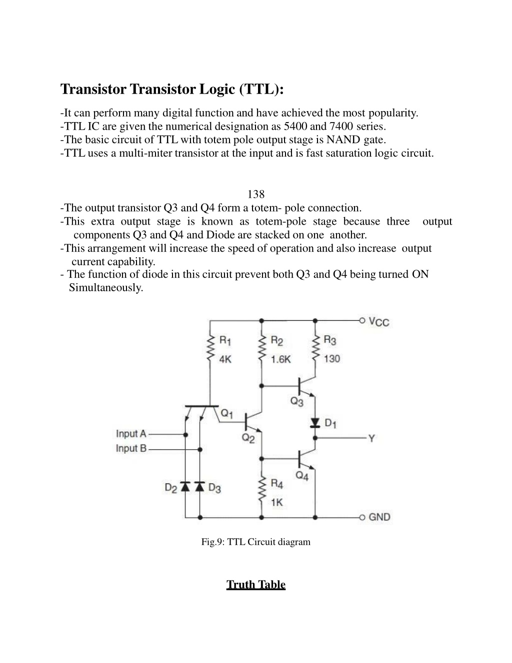
TransistorTransistor Logic (TTL): -It can perform many digital function and have achieved the most popularity. -TTLIC are given the numerical designation as 5400 and 7400 series. -The basic circuit of TTLwith totem pole output stage is NAND gate. -TTLuses a multi-miter transistor at the input and is fast saturation logic circuit. 138 -The output transistor Q3 and Q4 form a totem- pole connection. -This extra output stage is known as totem-pole stage because three components Q3 and Q4 and Diode are stacked on one another. -This arrangement will increase the speed of operation and also increase output current capability. - The function of diode in this circuit prevent both Q3 and Q4 being turned ON Simultaneously. output Fig.9: TTL Circuit diagram Truth Table
A B Y= ? . ? 0 0 1 0 1 1 1 0 1 1 1 0 139 Operation: A= 0, B= 0; A= 1, B= 0; A= 0, B=1; -The emitter base junction of Q1 turns on. -The collector potential of Q1 falls to 0v,then Q2 turns off. -Therefore, at point M we have 0 volt i.e., the base voltage of Q2 is 0 volt. -So that, Q2 is also turns off. -But at the same time we have L=+VCC, this voltage is applied on the base of Q4 -As a result transistor Q3 is turned ON. -Therefore, the output voltage is given by: V0= +VCC- [Voltage drop in R4+drop in diode D ] -A=1, B=1; -When becomes - However its collector base junction is forward bias, supplying base current to the transistor Q2. Hence Q2 turns ON. - As a result collector potential of Q2 becomes "0" volt. - Now if L= 0 volt is applied to the base of Q3, it turns off. - At the same time Q4 is turn ON. Then its collector potential nearly equal to 0volts. - Hence the output is low or logic 0. both input are high then emitter base junction of transistor Q1 reverse bias. Hence Q1 is turned off.
Characteristics: TTL has greater speed than DTL. Less noise immunity. Power dissipation is 10mw. It has fan-in of 6 and fan-out of 10. Propagation time delay is 5-15nsec. 140 Comparison of TTL Logic gates Power dissipation (mw) Speed Power Product Propagation delay Name Abbreviation (PJ) (ns) Standard TTL TTL 10 10 100 Low Power TTL LTTL 33 1 33 High Speed TTL HTTL 6 22 132 SchottkyTTL STTL 3 19 57 Low Power SchottkyTTL LSTTL 9.5 2 19 Note: The standard TTL gate was constructed with different resistor values to produce gate with lower dissipation or higher speed.
The propagation delay of a saturated logic family depends largely on two factors, storage time and RC time constant. Example 5: A two input NAND gate has Vcc = +5 V and 1 K load connected to its output. Calculate the output voltage, (a) When both input are LOW (b) When both input are HIGH. Solution: a) When both inputs of NAND gate are LOW, the output is HIGH and it is given as, VOH = VCC VCE(sat)- VD - IL x(130 ) = 5 - 0.1 - 0.7 - IL(130 ) = 4.2 V - IL(130 ) where the load current is, IL= VOH =VOH RL 1K 141 Substituting in the equation 1 we get, = 4.2V -VOH(130 ) V OH 1K 130???=4.2 V + OH 1000 1130V VOH=4200 4200 1130=3.716V VOH= b) When both inputs of NAND gate are HIGH, the output is LOW and it is given as, VOL = VCE(sat) = 0.1V
