Exploring Nanofabrication: Revolutionizing Technology at the Nano Scale
Nanofabrication is a cutting-edge technology that manipulates materials on a minuscule scale, smaller than 100 nm. This process enables the creation of intricate structures like semiconductor chips, lab-on-a-chip devices, and mimicking natural nanostructures. With examples like the Apple A7 chip containing over 1 billion transistors, nanofabrication showcases the incredible potential to revolutionize industries by scaling down complex systems to the nano level. By mimicking nature's nanostructures and shrinking clinical labs to handheld sizes, nanofabrication is pushing the boundaries of imagination.

Download Presentation

Please find below an Image/Link to download the presentation.
The content on the website is provided AS IS for your information and personal use only. It may not be sold, licensed, or shared on other websites without obtaining consent from the author. Download presentation by click this link. If you encounter any issues during the download, it is possible that the publisher has removed the file from their server.
E N D
Presentation Transcript
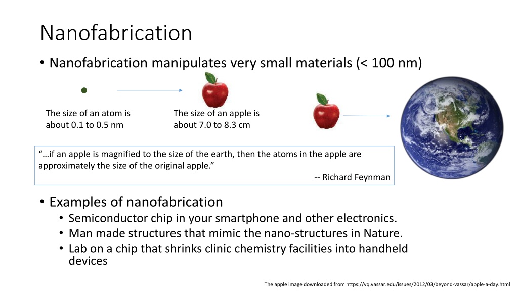
Nanofabrication Nanofabrication manipulates very small materials (< 100 nm) The size of an atom is about 0.1 to 0.5 nm The size of an apple is about 7.0 to 8.3 cm if an apple is magnified to the size of the earth, then the atoms in the apple are approximately the size of the original apple. -- Richard Feynman Examples of nanofabrication Semiconductor chip in your smartphone and other electronics. Man made structures that mimic the nano-structures in Nature. Lab on a chip that shrinks clinic chemistry facilities into handheld devices The apple image downloaded from https://vq.vassar.edu/issues/2012/03/beyond-vassar/apple-a-day.html
Nanofabrication makes microelectronic chips Transistor, the on/off switch Apple A7 chip includes over 1 billion transistors on a die 102 mm2 in size. 1138 nm Transistor-Level Image of the Apple A7 Chipworks
Microelectronic chips have billions of nano-transistors Phil. Trans. R. Soc. A (2012) 370, 3950 3972 Imagine building 1 billion houses, including their water, gas, sewage, telephone lines, cables, roads, and highway systems all on your finger nail. How would you do it? Cu metallization characteristic of a six-level structure associated with a production 32- bit RISC Processor in the CMOS 7S technology. (Courtesy of T Way, IBM Microelectronics Division, Burlington, VT.)
The nanostructure on the butterfly wing can be mimicked using nanofabrication Blue Morpho butterfly Radwanul H. Siddiquea, Karlsruhe Institute of Technology proceedings.spiedigitallibrary.org Rene Lopez, UNC at Chapel Hill Journal of Vacuum Science & Technology B 30, 061802 (2012);
Nanofabrication can shrink clinical chemistry laboratories to the size of handheld devices Nanofabrication can shrink clinical chemistry laboratories to the size of handheld devices Clinical lab to handheld device enabled by nanofabrication http://www.royalwolverhamptonhospitals.nhs.uk/pathology_services/departments/clinical_chemistry.aspx http://www.siliconsemiconductor.net/article/75748- Commercialising-Lab-On-A-Chip-Technology.php
Nanofabrication is only limited by our imagination http://www.zyvexlabs.com/EIPBNuG/EIPBN2007/2007.html
Photolithography: A key process to make small things over large areas Create a Designed pattern on a transparent substrate (Mask) Put photoresist on wafers Shine a light to change the photoresist The pattern replicated in photoresist after developer wash (Cartoons taken from ASML presentation slides)
Positive photoresist and negative photoresist UV light Mask blocks UV light at some areas Photoresist only exposed where UV passes Substrate Light increases solubility in positive resist Light decreases solubility in negative resist
How can light change a materials solubility Light is electromagnetic radiation with energy Ep=h Absorption of electromagnetic radiation can move an electron to an excited state, which may trigger a chemical change. When the electromagnetic radiation is strong enough, the absorption of the radiation can directly remove an electron from the molecule, which is a chemical change. The chemical changes can change material s solubility. Ionization n=3, E3 n=2, E2 Electron in an excited state or n=1 , E1 Absorption of electromagnetic radiation E = h nucleus Chm.1.1.3 Explain the emission of electromagnetic radiation in spectral form in terms of the Bohr model.
An example of positive photoresist Photoresist before exposure to UV light + Insoluble in base solution UV light + H2O Photoresist after exposure to UV light + Soluble in base solution
An example of negative photoresist All negative photoresists function by light induced cross-linking of a photosensitive agent. By cross-linking the long polymer chain the solubility in the developer is reduced. J. Chem. Educ., 1979, 56 (8), p 541 http://pubs.acs.org/doi/abs/10.1021/ed056p541