Electric Field Distribution in Vacuum Nano-Diode

Growing interest in miniaturization of anode-cathode gap using fine emission tips for vacuum nano-diode applications. This study investigates the effects of finite AK gap on electric field distribution around emission tips, utilizing Schwarz-Christoffel transformation. Insights from this research have implications for energy harvesting and conversion in solar cells.

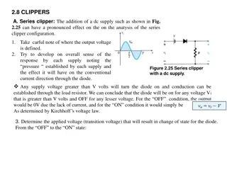
Download Presentation

Please find below an Image/Link to download the presentation.
The content on the website is provided AS IS for your information and personal use only. It may not be sold, licensed, or shared on other websites without obtaining consent from the author. Download presentation by click this link. If you encounter any issues during the download, it is possible that the publisher has removed the file from their server.
E N D
Presentation Transcript
Field distribution in a vacuum-nano diode Jinpu Lin, and Peng Zhang Department of Nuclear Engineering and Radiological Science University of Michigan, Ann Arbor 6? MIPSE Graduate Student Symposium Ann Arbor, MI October 7, 2015 Work Supported by AFOSR Grant No.FA9550-14-0309 1
Introduction There is growing interest in miniaturization of anode-cathode (AK) gap by using fine emission tips to realize a vacuum nano-diode, showing great potential for energy harvesting and conversion in solar cells.1 [2] A sharp anode tip sufficiently close to the flat graphene surface induces electron emissions from graphene surface.3 Existing models usually assume that the emission tip is far away from the anode, whose effect on tip field enhancement is thus ignored. We study the effects of finite AK gap on the electric field distribution on and around an emission tip, using Schwarz- Christoffel transformation. [1]. F. Yesilkoy, et al, A Mid-IR Antenna Integrated with a Geometrically Asymmetrical Metal-Insulator-Metal Rectifying Diode, in Rectenna Solar Cells, G. Moddel and S. Grover, Eds. Springer New York, 2013, pp. 163 188. [2]. P. Zhang, and D. Hung, An analytical model for ballistic diode based on asymmetric geometry , J. Appl. Phys., 115, 204908 (2014). [3]. S. Santandrea, et al, Field emission from single and few-layer graphene flakes, Appl. Phys. Lett., 98, 163109 (2011). 2
Schwarz-Christoffel Transformation.4 Z w Mapping from polygonal boundaries (z-plane) onto real axis of the w- plane. We can then transform the points on emission tip into points on a straight line. [4]. F.B. Hilderbrand, Advanced Calculus for Applications (Printice-Hall, New Jersey, 1962) 3
Schwarz-Christoffel Transformation for AK gap with a trapezoide tip Z H A B v W ?3 ?4 ?3 - ?4 0+ 1 - 0 d ?1 ?2 u D ?1 ?2 F G B C A H a y h G C z D F a= half width of tip h=depth of tip d=distance of gap ?= acute angle of tip The transformation formula is given below: ?? ??= ? ? 1? 1 ? ? ? ? ?3 ? ? ? ?4 ? ? ? ?3 ? 4
Schwarz-Christoffel Transformation for AK gap with a trapezoide tip ? ? ? ? ?1 ? ?3 ? ?3 ? = ? ?? + ?0 ? ? ? ? ? ? 1 ? ?4 ?0 ???? (0 ,0) (0+,0) Point B [ , ?] Point ? Point D [ ? cot?, 0] Point ?1 Point ?2 [ , 0] (1, 0) [ ?, ] (?3,0) ,0) [?, ] (?3 ???3 ?? ?3?3 ??? ?3 ?? ?3?3 ? ? ?? ???? ?? ???? ? ?3 2?? ? ?3 ? ? 1 ?3 ? ?3 ? ? 1 ? = ?= ? For any given ?, we can calculate ?3,?3 ? ?, ?, ,??? ?4. ?3 ? ?= ? sin? ?4= ?3?3 1 , 5
Example: ?3 & ?3 ??.?/ (? ?? ?????) 2 = ?3 ?3 6
Example: ?3 & ?3 ??.?/ ( ? ?? ?????) a/h=0.1 ? = ?/2 ? = ?/3 ? = ?/4 ? = ?/6 ? = ?/2 ? = ?/3 ? = ?/4 ? = ?/6 ?3 ?3 7
E-field calculation ? ? = ???0log ? ?? ???= ?? ?? ?? ?? ?? ??= ?? ? 1 ? ?3 ? ?4 ? ?3 ?? ???= ??0 As w ,?? ???= ??0 As w 0, ?? ???= ??0 Far away from the tip, uniform electric field is recovered. 8
Example: E vs. z/h ? = 0.1,? =? 2 Along ???1?2?? ? ?0 ? ?0 Electric field is enhanced near the tip when d/h is decreased. Field enhancement is found at both cathode and anode. 9
Current Emission and Field Enhancement Factor A1 B1 Consider Field Emission induced current: 2exp( ??? ? ? = ?FN(?2?0 ? ?0)) [ ?2] ???=1.5 10 6 exp(10.4 ?), 3 2, ? ???= 6.44 109? ?0=?? ?, ? ???? ???????? ?? ? = ????? ?? ???????? ??????, 10
Current Emission and Field Enhancement Factor A1 B1 Average current emitted from the tip ??1?2? is: 2? exp ??? ??? ??1?2??? ?? ??? ?1???= , ?? ?? = ? + 2 cot? , ??(?) = local electric field at point s along the surface ??1?2? . Average current emitted from the flat surface ?1?1 is: 2? exp ??? ??? ?1?1?? ?? ??? ?2???= , ?1?1 ?1?1=DF, ??? = local electric field at point s along the surface ?1?1. Field Enhancement Factor is obtained from: ??? ?1,2 ?0))?1,2 2 2exp( ?1,2= ???(?1,2 ?0 11
Field enhancement factor ? vs. d/h a/h=0.1, ? =? 2,?0= 3 108? ?,? = 4 ?? ?2 ?1 As the normalized gap space d/h decreases (<2), both ?1 ??? ?2 ????????? ?????????????. AS d/h>5, ?1 ??? ?2 converges to constant values, corresponding the case of d/h 12
Field enhancement factor ? vs. a/h d/h=2, ? =? 2,?0= 3 108? ?,? = 4 ?? ?2 ?1 As a/h increases, ?1 ?????????,??? ?2 ?????????. 13
Field enhancement factor ? vs. ?/h a/h=0.1, ? = 4,?0= 3 108? ?,? = 4 ?? ?2 ?1 As ? increases, ?1 ?????????,??? ?2 ?????????. 14
Field enhancement factor ? vs. ?0 a/h=0.1? =? 2,? = 2,? = 4 ?? ?2 ?1 ?0 [? ?0 [? ?] ?] As ?0increases, ?1 ?????????. ?2 is insensitive to ?0. 15
Summary & future work We calculated the local electric field inside the gap with a single trapezoid tip, by using the Schwarz-Christoffel Transformation. We evaluated the effective field enhancement factor for field emission, for both electrode with a tip and the flat electrode. Investigate tips of other shape, like semi-circle. Investigate multiple tips for electron emission. Compare the results with experiments. 16