Understanding Conductivity and Current in Extrinsic Semiconductors
This content delves into the intricacies of conductivity in extrinsic semiconductors, exploring the behavior of carriers in n-type and p-type materials. It covers topics such as drift current density, diffusion current density, the Einstein relation, recombination, and the Hall effect. Practical examples and solutions are provided to aid in comprehending these fundamental concepts in electronic physics.
Download Presentation

Please find below an Image/Link to download the presentation.
The content on the website is provided AS IS for your information and personal use only. It may not be sold, licensed, or shared on other websites without obtaining consent from the author. Download presentation by click this link. If you encounter any issues during the download, it is possible that the publisher has removed the file from their server.
E N D
Presentation Transcript
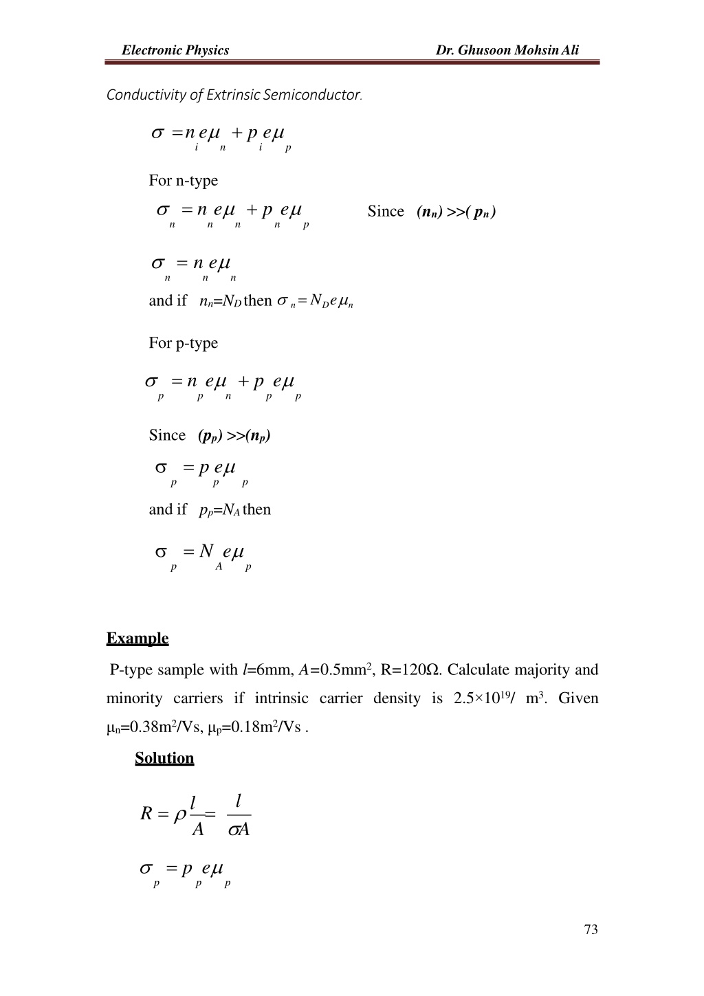
Electronic Physics Dr. Ghusoon MohsinAli Conductivity of ExtrinsicSemiconductor. =ne + p e i n i p For n-type = n e + p e n n Since (nn) >>( pn) n n p = n e n and if nn=ND then n = NDe n n n For p-type = n e + p e p p n p p Since (pp) >>(np) = p e p p p and if pp=NAthen = N e p A p Example P-type sample with l=6mm, A=0.5mm2, R=120 . Calculate majority and minority carriers if intrinsic carrier density is 2.5 1019/ m3. Given n=0.38m2/Vs, p=0.18m2/Vs . Solution l R = l= A A = p e p p p 73
Electronic Physics Dr. Ghusoon MohsinAli 2 ni =np pp = p = 100= 3.46 1021/m3 1.6 10 19 0.18 p e p p n2 n =i= 1.9 1017 / m3 p p p Drift Current Density An electric field is applied to a semiconductor will produce forceon electrons and holes so that they will experience a net acceleration and net movement. This net movement of charge due to an electric field is called drift. The net drift of charge gives rise to a drift current. The current density due to electrons drift J = ne E n n The current density due to electrons drift J = pe E p p The total current density due to electrons and holes drift J = J + J = ne E + pe E n p n p Example Calculate the drift current density in a gallium arsenide sample at T=300 K, with doping concentration Na=0, Nd=1022/m3, n=0.85m2/V.s, p=0.04m2/V.s, E=10 V/cm, ni=2.2 1017/m3. Solution 74
Electronic Physics Dr. Ghusoon MohsinAli Since ND>>Na then it isn-type n N N n A D n 1022 /m3 The minority hole concentration is n2 p =i= 3.24 102 / m3 n J =( 1.6 10 19) (0.85)( 1022)( 103)=136 104A/ m2 Diffusion Current Density It is gradual flow of charge from a region of high density to a region of low density. Current density due to electron diffusionis J = eDdn ndx n Current density due to hole diffusion is J = eDdp pdx p Where Dn, Dp (cm2/s) are electron and hole diffusion constants, respectively. dn dx dp dx Density gradient of electrons Density gradient of holes 75
Electronic Physics Dr. Ghusoon MohsinAli Total Current Density The total current density is the sum of these four components J = en E + ep E + eDdn eDdp n dx pdx n p EinsteinRelation This relation between the mobility and diffusion coefficient. D D kT n= p = e n p D =kT = e 39 Example Determine the diffusion coefficient, assume the mobility is 1000cm2/V.s at T=300K. Solution D =kT = 0.0259 1000 = 25.9cm2 /s e Rcombination Recombination that result from the collision of an electron with a hole. This process is the return of a free electrons in the conduction band to valence band, there is a net recombination rate by difference between the recombination and generation rates. D D L = L = n n p p Where L the distance traveled by charge carrier before, recombination life time. 76
Electronic Physics Dr. Ghusoon Mohsin Ali Hall Effect: As shown there is a current Ix resulting from an applied electric field Ex in x- direction an electrons will drift vx. A magnetic field By (wb/m2) is superposed on applied electric field Ex , whereby the current Ix and the magnetic flux By are perpendicular to each other. The electrons will experience a Lorentz force Fzperpendicular to Ixand By( in z direction) F = ev B z x y Thus the electrons under the influence of this force will tend to crowds one face in the sample. This collection of electrons to one side establish an electric field in z-direction is known Hall effect EH or Ez. Resulting a voltage VH between the upper and the lower faces of the sample is observed: On the other hand eE = ev B z x y the current density Jx is givenby: E = v B J = nev x Jx = Ex z x y x VH Fig. 5.7. Hall measurementsituation 77
Electronic Physics Dr. Ghusoon MohsinAli J E =xB ne z y I I = x= A Jx x bd Hall coefficient H=1 R Where n is the total number of charge carrier per volum ne I E = R xB Hbd z y I VH=R xB b Hbd y I V = R H xB d y H I n = B x V ed y H Where all the quantities in the right-hand side of the equation can n measured. Thus the carrier concentration and carrier type can e obtained directly from the Hall measurement. J = E =ne E x x x ne V I x= x A L 78
Electronic Physics Dr. Ghusoon MohsinAli I L = x neV A x Example Determine the majority carrier concentration and mobility, sample 10-1cm length and 10-2 10-3cm2cross section area, given Hall effect parameters Ix=1mA, Vx=12.V, B=5 10-2tesla, VH=-6.25mV. Solution The negative Hall voltage indicate n-type semiconductor I n = B x V ed y H (10 3)(5 10 2) 3 n = = 5 10 m 21 (1.6 10 19)(10 5)( 6.25 10 3) I L = x neV A x (10 3)(10 3) = = 0.1m /V.s 2 (1.6 10 19)(5 1021)(12.5)(10 4)(10 5) 79
Electronic Physics Dr. Ghusoon Mohsin Ali Problems Q1: Calculate the drift current density in silicon sample. If T=300 K, Nd=1021/m3, Na=1020/m3V, n=0.85m2/V.s, p=0.04m2/V.s, E=35 V/cm.. (Ans: 6.8 104A/m2). Q2: A cubic doped n-type silicon semiconductor sample at T=300 K, n=0.85m2/V.s, R=10k , J=50A/cm2 when 5V is applied.Calculate ND. . Q3: Determine 10mm 1mm 1mm sample, a magnetic field 0.2wb/m2 is superposed on applied voltage 1mV. Calculate Hall voltage if electrons density 7 1021/m3 n=0.4 m2/Vs. 80
