Understanding Stick Diagrams in VLSI Circuit Design
Stick diagrams in VLSI design help visualize the layout of components on silicon by capturing topography and layer information through color codes or monochrome encoding. They serve as an interface between symbolic circuits and actual layouts, facilitating the planning of layout and routing while depicting relative component placement. Stick diagrams do not display exact component placement or low-level details such as transistor sizes or wire specifics, but they assist in layout design and routing decisions.
Download Presentation

Please find below an Image/Link to download the presentation.
The content on the website is provided AS IS for your information and personal use only. It may not be sold, licensed, or shared on other websites without obtaining consent from the author. Download presentation by click this link. If you encounter any issues during the download, it is possible that the publisher has removed the file from their server.
E N D
Presentation Transcript
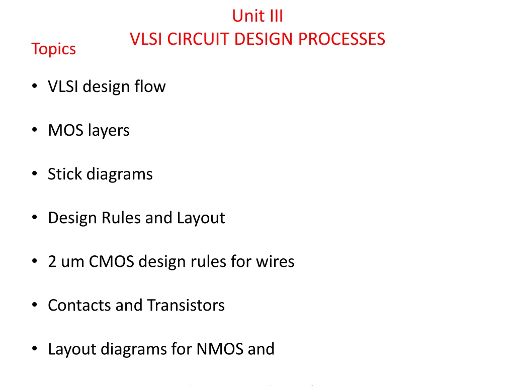
UnitIII VLSICIRCUITDESIGNPROCESSES Topics VLSI design flow MOS layers Stick diagrams Design Rules and Layout 2 um CMOS design rules for wires Contacts and Transistors Layout diagrams for NMOS and CMOS inverters and gates, Scaling of MOS circuits
VLSI Design of approach of IC 6 2/ 03 8/2015
LayerTypes p-substrate n-well n+ p+ Gate oxide (thin oxide) Gate(polycilicon) Field Oxide Insulatedglass Provide electrical isolation
Stick diagram Encodings for a simple single metal nMOS process COLOR LAYERS MASK LAYOUT ENCODING CIF LAYER STICK ENCODING MONOCROME MONOCROME n- diffusion N D GREEN n+active NP Thniox Polysilicon RED N M BLUE BLACK Metal 1 N C N G GRAY Contact cut Overglass NI nMOS ONLY NOT APPLICABLE Implant YELLO W nM OS ONLY NB Buried contact BROWN
Stick Diagrams Metal poly ndiff Buried Contact Can also draw in shades of gray/line style. pdiff Contact Cut
StickDiagrams VLSI design aims to translate circuitconcepts onto silicon. Stickdiagrams are a means ofcapturing topography and layer information using simple diagrams. Stickdiagrams convey layer information through colour codes (or monochrome encoding). Acts as an interface between symbolic circuit and the actual layout. Does show all components/vias. It shows relative placement of components. Goes one step closer to the layout Helps plan the layout and routing
Stick Diagrams Does not show Exact placement of components Transistor sizes Wire lengths, wire widths, tub boundaries. Any other low level details such as parasitics.. Does show all components/vias. It shows relative placement of components. Goes one step closer to the layout Helps plan the layout and routing
StickDiagrams Some rules Rule 1. When two or more sticks of the same type cross or touch each other that represents electrical contact. Rule 2. electrical contact. (If electrical contact is needed we have to show the connection explicitly). When two or more sticks of different type cross or touch each other there is no
Stick Diagrams Stick Diagrams Some rules Rule 3. transistor. When a poly crosses diffusion it represents a Note: If a contact is shown then it is not a transistor.
Stick Diagrams Stick Diagrams Some rules Rule 4. touching of p-diff with n-diff. All pMOS must lie on one side of the line and all nMOS will have to be on the other side. In CMOS a demarcation line is drawn to avoid
NMOS INVERTER 5 V 5 v Dep Vout Enh Vin 0 V 0V
NMOS-NOR 6/3/2015 222
NMOSEX-OR 6/3/2015 223
NMOSEX-NOR 6/3/2015 224
PMOS-INVERTER 6/3/2015 225
PMOSNAND 6/3/2015 226
PMOS-NOR 6/3/2015 227
SticksdesignCMOSNAND: Start with NAND gate: 6/3/2015 228
NANDsticks VDD a out b VSS 229 6/3/2015
Stick Diagram - Example A OUT B NOR Gate 6/3/2015 230
Stick Diagram - Example Power Out A C B Ground 6/3/2015 231
2 I/P OR GATE 6/3/2015 232
2 I/P AND 6/3/2015 233
6/3/2015 234
Y=(AB+CD) 6/3/2015 235
Y=(AB+CD)STICK 6/3/2015 236
