Understanding Shift Registers in Sequential Logic Circuits

Shift registers are sequential logic circuits used for storing digital data. They consist of interconnected flip-flops that shift data in a controlled manner. This article explores different types of shift registers such as Serial In - Serial Out, Serial In - Parallel Out, Parallel In - Serial Out, Parallel In - Parallel Out, and bidirectional shift registers. The concept of a shift register counter is also discussed, along with practical examples and diagrams illustrating their operation.

Download Presentation

Please find below an Image/Link to download the presentation.
The content on the website is provided AS IS for your information and personal use only. It may not be sold, licensed, or shared on other websites without obtaining consent from the author. Download presentation by click this link. If you encounter any issues during the download, it is possible that the publisher has removed the file from their server.
E N D
Presentation Transcript
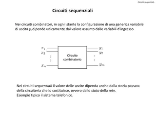
SHIFT REGISTERS Introduction : Shift registers are a type of sequential logic circuit, mainly for storage of digital data. They are a group of flip-flops connected in a chain so that the output from one flip-flop becomes the input of the next flip-flop. Most of the registers possess no characteristic internal sequence of states. All the flip-flops are driven by a common clock, and all are set or reset simultaneously. In this chapter, the basic types of shift registers are studied, such as Serial In - Serial Out, Serial In - Parallel Out, Parallel In - Serial Out, Parallel In - Parallel Out, and bidirectional shift registers. A special form of counter - the shift register counter, is also introduced.
Serial In Serial In - - Serial Out Shift Registers Shift Registers Serial Out A basic four-bit shift register can be constructed using four D flip- flops, as shown below. The operation of the circuit is as follows. The register is first cleared, forcing all four outputs to zero. The input data is then applied sequentially to the D input of the first flip-flop on the left (FF0). During each clock pulse, one bit is transmitted from left to right. Assume a data word to be 1001. The least significant bit of the data has to be shifted through the register from FF0 to FF3.