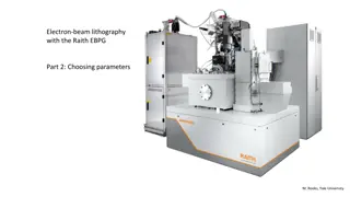
Understanding Proximity Effect in Electron Beam Lithography
Explore the impact of proximity effect in EBL, its causes, and its effects on resolution. Learn about physical models, reduction techniques, and correction methods to mitigate proximity effect and enhance lithographic precision.
Download Presentation

Please find below an Image/Link to download the presentation.
The content on the website is provided AS IS for your information and personal use only. It may not be sold, licensed, or shared on other websites without obtaining consent from the author. Download presentation by click this link. If you encounter any issues during the download, it is possible that the publisher has removed the file from their server.
E N D
Presentation Transcript
Proximity Effect in EBL Jian Wu Feb. 11, 2014
Outline Introduction Physical and quantitative model of proximity effect Reduction and correction of proximity effect Conclusion
Introduction Proximity effect: Electron scattering effect. Non-uniform exposure. Causing exposure of areas surrounding the area where the electron beam is incident. Limiting the resolution in EBL.
Forward and Backward Scattering Resist Resist Substrate Substrate Forward scattering: - Small angle. - Inelastic. - Generating secondary electrons with low energy. Backward scattering: - Large angel. - Elastic. - High energy, same range of primary electrons. - Large travel length. Backscattering is mainly responsible for resist exposure far from incidence (proximity effect), as BSE can generate SE along its path to expose the resist there.
Energy Density Profile 2 2 +h 1 1 a2exp -r r f (r)= b2exp - (1+h)p a b : range of forward scattering (in m) : range of backscattering (in m) : ratio of backscattering to forward scattering forward scattering backward scattering - Energy density profile deposited in resist layer due to a point or pixel exposure. - Approximated by the sum of two Gaussian distributions. - Used in proximity effect correction algorithm.
Reducing Proximity Effect Electron beam energy & resist thickness df=0.9(Rt/Vb)1.5 dfis the effective beam diameter in nm Rtis the resist thickness in nm Vbis the beam voltage in kV - - High electron beam energy Thin resist thickness
Reducing Proximity Effect Multilayer resists The upper layer is used for patterning. The lower layer functions to reduce backscattering. the resolution increases considerably. The disadvantage is the increased process complexity.
Proximity Effect Correction Dose modification - - Not using the same dose for the whole pattern. Changing the dose in some parts of the pattern. Shape modification - - - A single dose is use for the entire pattern. Reducing structure size for exposure compensation. Changing the shapes at critical points. Background exposure correction - - Writing a second exposure which is the inverse of the intended image. Background dose is brought to a constant level.
Conclusion Electron scattering (forward and backward) is responsible for proximity effect. High electron beam energy should be used to obtain high resolution. Algorithms can correct proximity effect. But there is a trade-off between speed, complexity and accuracy.
References [1] http://nanolithography.gatech.edu/proximity.htm [2] Chang, T. H. P. (1975). "Proximity effect in electron-beam lithography. Journal of Vacuum Science and Technology 12(6): 1271-1275. [3] Nanofabrication: principles, capabilities and limits, by Zheng Cui [4] G. Owen, Methods for proximity effect correction in electron lithography, Journal of Vacuum Science Technology B, 8(6), 1889-1892, 1990


