Optimizing E-Beam Design: Settling Time and Avoiding Costly Mistakes
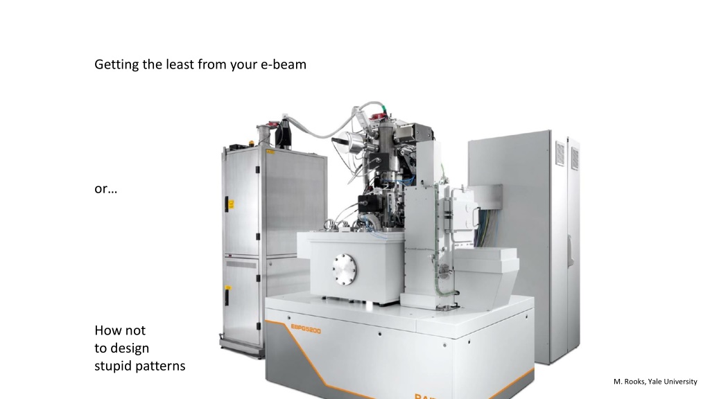

Getting the least from your e-beam
or…
How not
to design
stupid patterns
M. Rooks, Yale University
Settle Down
Now that you have completed the CAD tutorial, you probably think
you can slap together your design and the e-beam system will poop
out a shiny nugget. Nope.
First, let’s think about
settling time
. Every shape requires the beam
to be deflected to a particular place, using a 20-bit main-field DAC
and a fast 14-bit subfield DAC. (You should know what a DAC is by
now, so go look it up.)
After one main-field deflection, the beam remains blanked for
~150µs while the beam position settles. (Or longer, if the deflection is
large.)
After one subfield deflection, the beam remains blanked for ~1 µs (or
longer) while the beam position settles.
For patterns with a lot of small shapes, this can really add up.
main deflector
~150 µs
subfield deflector
~1 µs
This is not a circle
This is a polygon with n sides. There is no such thing as a circle in
e-beam land. The number of sides matters a lot, because the use of
more sides requires the use of more small shapes to generate the
pattern.
This means the deflection settling time will increase dramatically
simply by using more vertices to define the polygon. After conversion
to gpf format, a “circle” could look like this…
…if we use 360 sides
…or like this if we use only 6 sides
200 nm
The diameter of this “circle” is 200nm. We
have converted it to gpf format using a 5nm
beam step size. When exposed at a high
enough dose, these two “circles” will look
exactly the same on the wafer.
BUT
The first one will have a settling time
overhead of
19 µs
and the second will have
a settling time of
3 µs
.
Actual size after exposure
and development
What you design is not what you get
3 mm
A 3 x 3 mm patch of these dots with a
pitch of 300nm (center-to-center spacing)
will contain 100 million polygons.
The total overhead for deflection settling
is
32 minutes
for the 360 sided shape, or
5 minutes
for the hexagon.
So being stupid will cost you some serious
money. In this case, it will cost ~ $50 more
for each pattern.
Why not reduce that dot down to one pixel?
That’s not a bad idea. You can bias a dot down to one pixel. If you
want to use a beam step size of 5 nm, then in the CAD program you
should draw a 5x5 nm box. The actual size of the dot will be
determined by the exposure dose and development chemistry.
In this case the concept of
“
dose
”
(in coulombs / cm
2
) is unclear.
Scattered electrons spread the energy over an area much larger than
the single pixel, but when you specify a
“
dose
”
the EBPG will
calculate the dwell time based on just 5x5 nm
2
. Empirically we find
that the dose should be set roughly 25 times higher than the dose for
a large shape.
Similarly, the dose for a single-pixel line will have to be roughly 5
times higher than the dose used for a large shape.
What you see
What you get
Here’s a neat trick: If you use a beam step size of
100nm then a rectangle exposed at a low enough
dose will end up as a set of dots! The beam will try
to fill in the rectangle by making 100nm hops –
without blanking or settling. The dots will be a bit
elongated, but this might not matter for your
application. In fact, making a field of “dots on the fly”
is a common diagnostic test. Misplacement of the
dots can be used to measure abnormal beam
deflection noise.
Dots in HSQ resist, using a single large
rectangle printed with a 80nm beam step
.
What you see
What you get
design
process bias
PMMA
silicon
e-
Shrinking and growing: Bias
The single-pixel dot is an example of ‘bias’. The exposure and
development process will broaden the shape. We could call
this a ‘positive’ process bias, or we could describe the pattern
has having a ‘negative’ size bias.
When using positive resist (eg PMMA) all shapes will be larger
than the design in the CAD files. Typically, a line in the resist
will widen by at least 10% of the resist thickness. For example,
if you use 3% PMMA for a thickness of 200nm, then you can
expect a process bias of about 20nm in the resist. If you use
this resist as an etch mask, then the width will increase
further.
It makes sense to design your pattern with smaller sizes; that
is, to bias the pattern.
Be prejudiced against bias
It’s tempting to design a device at the correct, unbiased size,
then shrink it by some amount right before you print it. You
could use Beamer, CATS, or Layout to apply an automatic bias.
The problem is that automatic biasing will often separate
shapes. You must be very careful to match adjoining vertices
(without overlaps) and you must put all the vertices on the
exposure grid. Otherwise, shapes will break apart.
You can avoid this problem by applying an overlap removal
step (aka “healing” in Beamer) but that step might take a long
time, and the process will wipe out all layer and datatype
settings.
Baising geometry automatically is a very difficult problem, and
so it’s not surprising that even the best software goofs it up
sometimes.
It’s a lot more reliable to put in a size bias yourself, by hand.
What you want
What you get
Unbiased design
with an overlap
More sides or fewer sides?
Will a smaller beam step make
smoother waveguides?
Shape settling overhead is a lot smaller when the polygons have fewer
vertices, but polygons that are supposed to be smooth – such as
waveguides – might not be smooth enough.
When choosing a beam step size, consider the fact that the intrinsic
lumpiness of PMMA is around 5nm, and that of HSQ is around 3nm.
Metal grain size or lack of etch selectivity will also cause 1-10nm more
roughness. Beam deflection noise adds several more nanometers.
Therefore there is no point in using a beam step size smaller than
about 5nm. If you need smoother features then you should be
thinking about desperate measures such as…
•
Improving the etch process
•
Annealing and reflow
•
Hydrogen plasma smoothing
•
Waveguide cladding material
If your device requires atomic smoothness, then it’s time to change
the entire concept of your device.
beam step = 5nm beam step = 50nm
Placement accuracy
The beam step size is always a multiple of the least significant bit,
LSB. On our EBPG the LSB is usually set to 1nm. Pattern features will
snap to multiples of the beam step size.
For example, to fabricate a Bragg grating on a GaAs laser we might
want a grating with a pitch (center-to-center) distance of precisely
241.3nm. Unfortunately, our e-beam LSB is normally set to 1nm,
which is not accurate enough.
In this example we could recalibrate the LSB to 0.7541nm, and we
could choose a beam step size which is 5 times the LSB, 3.7703nm.
This makes the grating pitch equal to 64 beam steps.
The EBPG system can be recalibrated with an arbitrary LSB. Other e-
beam systems achieve the same “field stretch” by
lying
about the
distance between alignment marks. A variety of different pitch values
requires recalibration with a variety of different LSBs (or different lies
about the mark positions.)
In practice, we almost never need to use a LSB other than 1nm
because we can allow periodic structures to snap to a coarse grid. It’s
the
average
pitch that matters.
DFB grating
241.3 nm = 64 beam steps
Photonic bandgap
cavity
Aperiodic Structures
Matching the deflection LSB to the grating periodicity will not
work if we need a continuum of grating pitches. For example, we
might need a
chirped
grating where the pitch varies from
1070.66nm to 1070.11nm over one millimeter. In this example we
cannot pick a convenient LSB.
Instead, we set the LSB to 1nm, then let the grating lines
snap
back and forth
onto the exposure grid. This coarse technique
works because light scatters weakly from each grating line, and
effectively averages over the placement errors.
Random snapping to a coarse grid is far easier and more versatile
than finding the perfect LSB. This is the preferred technique for
creating ‘weak’ gratings.
Chirpped dispersion filter
Oh Snap!
The previous slide made random grid snapping sound great. It
is
great for weak
gratings, but for everything else,
it’s terrible
. Here is an example of an array of
square rings, designed on a 10 nm grid, but converted to e-beam format with a 12
nm beam step size.
The rings have a 450 nm pitch, but because the 20 nm wide lines were designed
as “paths,” the edges of the lines fall on a 10 nm grid.
The linewidth is nominally 20 nm, but you can see that grid snapping to a 12 nm
beam step causes the linewidth to vary between 0 and 2 pixels. The exposure
would be very non-uniform.
The designer
should
have placed the array on a 12nm grid, and
should
have made
the linewidth a multiple of 12 nm. (Of course, she could have used a 10nm beam
step size instead.)
This example also illustrates the folly of using paths instead of polygons. If the
path corners are interpreted as being round, then those little corner fill shapes
can be lost by snapping to a coarse grid. It is smarter to convert paths to polygons
before saving the CAD file.
In this example, 20 nm wide lines exposed with a 12 nm beam step will be only
one pixel wide. In other words, they are “single pass” lines.
The moral of the story is: Design your pattern so the vertices are on the beam
step grid.
CAD file contains 20nm wide ‘paths’ at 450nm pitch.
Line edges fall on a 10nm grid. The square-ness of the
corners depends on how the file is saved.
After conversion to e-beam format using a 12nm beam step.
Corner pieces were lost because paths were interpreted as having
rounded corners. Line widths vary between 0 and 2 pixels.
But wait – what if the shapes are bigger?
Normally we try to make polygon vertices fall on the beam
stepping grid. BUT if the shapes are more than a few beam
steps wide, then we can relax this restriction.
It is possible to specify a
placement accuracy
which is smaller
than the beam stepping distance. Then the vertices of
polygons will fall on the finer placement grid, while the
shape is filled in with a larger beam step. What? How can the
electron beam hit both sides of such a shape?
The system will fill the shape cleverly, possibly with multiple
trapezoids, allowing some overlap in the center. This strategy
is called “split and bury.”
If the shape is only one to three pixels wide, then this trick
will not work.
As designed, the
vertices of this hexagon
fall on a 1 nm grid.
However, we want to
expose the shape with
a 10 nm beam step.
If the conversion
software (Beamer) is
given the freedom to
use a placement
accuracy of 1 nm, then
it will try to put the
beam shots on the
edges of the polygon;
that is, on a 1 nm grid.
Some overlaps are
allowed inside the
shape.
A few more common mistakes:
Tone reversal & overlaps
Reversing tone
Sometimes you need the “reverse” of a
pattern. For example, when creating
waveguides, you may wish to leave resist on
the pattern, so that most of the material will be
etched.
Reversing the pattern with software is probably
the wrong approach. Instead, you should be
using a negative resist such as HSQ or MA-n.
Probably
. We will talk about software pattern
reversal on the next slide.
The lesson of this slide is: USE THE RIGHT
RESIST. Use positive resist when you need slots
or holes. Use negative resist when you need to
etch away everything except your pattern.
Some people fall in love with the wrong resist,
and are afraid to switch. Or maybe they are just
too lazy. It’s sad to watch people waste so
much time. This advice probably applies to
more than just e-beam resist. Who knows.
e-
PMMA
Good:
this is
the right way
to use positive
resist
e-
Bad:
The wall
of positive
resist will fall
down or wash
away.
e-
Good:
this is
the right way
to use negative
resist
e-
Bad:
The slot
between
exposed
sections will
fill in.
HSQ
HSQ
Reversing tone in software
There are some odd cases where it is actually
faster to expose positive resist
around
the device.
Let’s assume that you have thought about negative
resist and you are not just being stupid.
You can reverse a pattern using Beamer, or with a
CAD program such as Layout or Design Workshop.
The process is usually found under “Boolean”
operations, where you must designate two shapes
and then do a “minus” or “not” operation.
The right way to define the second shape is to copy
your pattern and then apply a large positive bias.
When the original pattern is subtracted from the
fat version, the margin will remain.
The wrong way to define the second shape is to
use a large rectangle, which results in a very large
exposure area. This seems like common sense,
right? But people can be amazingly stupid. Not you
though.
Watch out: Sometimes even Beamer (!) will make
mistakes. Be sure to inspect the pattern carefully.
Wrong:
subtracting
the pattern from a
large rectangle
Right:
subtracting
the pattern from an
expanded version
of the same pattern
Overlaps
When you are designing things in a hurry, as usual, it is
tempting to let shapes overlap, as in this example. But watch
out! Wherever there is an overlap, the resist will be exposed
twice, doubling the exposure dose.
On the large pads, separated by 100 µm, this does not
matter. In the center, where narrow wires are separated by
100nm, this matters a lot. Sloppy CAD work in the center will
cause the wires to short together. Remember that the 1/e
distance for electron scattering in silicon is ~ 26 µm.
You could use a CAD program to remove these overlaps. In
Layout, use Utilities
Global Tools
Remove Overlap.
Or you could remove the overlaps with Beamer, in the
“Heal”
module.
BUT if you are using layers or datatypes to designate
different
doses
, then the doses will be lost when the
overlaps are removed. It is a lot smarter to avoid overlaps by
snapping to a convenient grid in the CAD program.
zoom
100 µm
0.5 µm
Overlaps on the
big pads cause
double exposures,
but this does not
matter at all.
Overlaps on the
narrow wires will
cause problems,
shorting the wires.
Finding overlaps with cview
It can be very difficult to see pattern overlaps, especially
if you have accidentally placed two copies of a cell in
one place, or if you have created an array with a pitch of
zero.
Often such problems are not found until you look at the
pattern in resist, and say “what happened?!”
That’s when you can look at the gpf pattern with
“cview,” which is one of the only ways to find overlaps.
By hovering the cursor over the pattern and pressing
the “Ctrl” key, you will get a report on all the shapes
under the cursor.
Two shapes are
under the cursor
Summary: Watch out for these stupid mistakes
•
Using too many vertices to define the unit cell of an array
•
Using a design grid which is not a multiple of the beam step (unless you have a good reason)
•
Setting the beam step below 5nm to decrease roughness
•
Choosing the wrong type of resist. Use positive to make holes, negative to make posts.
•
Including sloppy or accidental overlaps
The End
Now you should proceed to the quiz.
Dive into the intricacies of E-beam lithography design, focusing on the crucial aspects of settling time, polygonal shapes over circles, and the impact of dot size on pattern generation efficiency. Learn how to minimize settling time, reduce costs, and maximize output quality in your E-beam designs.

Download Presentation

Please find below an Image/Link to download the presentation.
The content on the website is provided AS IS for your information and personal use only. It may not be sold, licensed, or shared on other websites without obtaining consent from the author. Download presentation by click this link. If you encounter any issues during the download, it is possible that the publisher has removed the file from their server.
E N D
Presentation Transcript
Getting the least from your e-beam or How not to design stupid patterns M. Rooks, Yale University
Settle Down Now that you have completed the CAD tutorial, you probably think you can slap together your design and the e-beam system will poop out a shiny nugget. Nope. First, let s think about settling time. Every shape requires the beam to be deflected to a particular place, using a 20-bit main-field DAC and a fast 14-bit subfield DAC. (You should know what a DAC is by now, so go look it up.) main deflector ~150 s After one main-field deflection, the beam remains blanked for ~150 s while the beam position settles. (Or longer, if the deflection is large.) subfield deflector ~1 s After one subfield deflection, the beam remains blanked for ~1 s (or longer) while the beam position settles. For patterns with a lot of small shapes, this can really add up.
This is not a circle This is a polygon with n sides. There is no such thing as a circle in e-beam land. The number of sides matters a lot, because the use of more sides requires the use of more small shapes to generate the pattern. This means the deflection settling time will increase dramatically simply by using more vertices to define the polygon. After conversion to gpf format, a circle could look like this if we use 360 sides or like this if we use only 6 sides
What you design is not what you get Actual size after exposure and development The diameter of this circle is 200nm. We have converted it to gpf format using a 5nm beam step size. When exposed at a high enough dose, these two circles will look exactly the same on the wafer. 3 mm BUT A 3 x 3 mm patch of these dots with a pitch of 300nm (center-to-center spacing) will contain 100 million polygons. The first one will have a settling time overhead of 19 s and the second will have a settling time of 3 s. The total overhead for deflection settling is 32 minutes for the 360 sided shape, or 5 minutes for the hexagon. 200 nm So being stupid will cost you some serious money. In this case, it will cost ~ $50 more for each pattern.
Why not reduce that dot down to one pixel? That s not a bad idea. You can bias a dot down to one pixel. If you want to use a beam step size of 5 nm, then in the CAD program you should draw a 5x5 nm box. The actual size of the dot will be determined by the exposure dose and development chemistry. Here s a neat trick: If you use a beam step size of 100nm then a rectangle exposed at a low enough dose will end up as a set of dots! The beam will try to fill in the rectangle by making 100nm hops without blanking or settling. The dots will be a bit elongated, but this might not matter for your application. In fact, making a field of dots on the fly is a common diagnostic test. Misplacement of the dots can be used to measure abnormal beam deflection noise. What you see What you get In this case the concept of dose (in coulombs / cm2) is unclear. Scattered electrons spread the energy over an area much larger than the single pixel, but when you specify a dose the EBPG will calculate the dwell time based on just 5x5 nm2. Empirically we find that the dose should be set roughly 25 times higher than the dose for a large shape. Dots in HSQ resist, using a single large rectangle printed with a 80nm beam step. Similarly, the dose for a single-pixel line will have to be roughly 5 times higher than the dose used for a large shape.
Shrinking and growing: Bias What you see The single-pixel dot is an example of bias . The exposure and development process will broaden the shape. We could call this a positive process bias, or we could describe the pattern has having a negative size bias. What you get When using positive resist (eg PMMA) all shapes will be larger than the design in the CAD files. Typically, a line in the resist will widen by at least 10% of the resist thickness. For example, if you use 3% PMMA for a thickness of 200nm, then you can expect a process bias of about 20nm in the resist. If you use this resist as an etch mask, then the width will increase further. design process bias e- PMMA It makes sense to design your pattern with smaller sizes; that is, to bias the pattern. silicon
Be prejudiced against bias It s tempting to design a device at the correct, unbiased size, then shrink it by some amount right before you print it. You could use Beamer, CATS, or Layout to apply an automatic bias. Unbiased design with an overlap The problem is that automatic biasing will often separate shapes. You must be very careful to match adjoining vertices (without overlaps) and you must put all the vertices on the exposure grid. Otherwise, shapes will break apart. You can avoid this problem by applying an overlap removal step (aka healing in Beamer) but that step might take a long time, and the process will wipe out all layer and datatype settings. Baising geometry automatically is a very difficult problem, and so it s not surprising that even the best software goofs it up sometimes. What you want What you get It s a lot more reliable to put in a size bias yourself, by hand.
More sides or fewer sides? Will a smaller beam step make smoother waveguides? Shape settling overhead is a lot smaller when the polygons have fewer vertices, but polygons that are supposed to be smooth such as waveguides might not be smooth enough. When choosing a beam step size, consider the fact that the intrinsic lumpiness of PMMA is around 5nm, and that of HSQ is around 3nm. Metal grain size or lack of etch selectivity will also cause 1-10nm more roughness. Beam deflection noise adds several more nanometers. Therefore there is no point in using a beam step size smaller than about 5nm. If you need smoother features then you should be thinking about desperate measures such as Improving the etch process Annealing and reflow Hydrogen plasma smoothing Waveguide cladding material beam step = 5nm beam step = 50nm If your device requires atomic smoothness, then it s time to change the entire concept of your device.
Placement accuracy The beam step size is always a multiple of the least significant bit, LSB. On our EBPG the LSB is usually set to 1nm. Pattern features will snap to multiples of the beam step size. 241.3 nm = 64 beam steps For example, to fabricate a Bragg grating on a GaAs laser we might want a grating with a pitch (center-to-center) distance of precisely 241.3nm. Unfortunately, our e-beam LSB is normally set to 1nm, which is not accurate enough. DFB grating In this example we could recalibrate the LSB to 0.7541nm, and we could choose a beam step size which is 5 times the LSB, 3.7703nm. This makes the grating pitch equal to 64 beam steps. The EBPG system can be recalibrated with an arbitrary LSB. Other e- beam systems achieve the same field stretch by lying about the distance between alignment marks. A variety of different pitch values requires recalibration with a variety of different LSBs (or different lies about the mark positions.) In practice, we almost never need to use a LSB other than 1nm because we can allow periodic structures to snap to a coarse grid. It s the average pitch that matters. Photonic bandgap cavity
Aperiodic Structures Matching the deflection LSB to the grating periodicity will not work if we need a continuum of grating pitches. For example, we might need a chirped grating where the pitch varies from 1070.66nm to 1070.11nm over one millimeter. In this example we cannot pick a convenient LSB. Instead, we set the LSB to 1nm, then let the grating lines snap back and forth onto the exposure grid. This coarse technique works because light scatters weakly from each grating line, and effectively averages over the placement errors. Chirpped dispersion filter Random snapping to a coarse grid is far easier and more versatile than finding the perfect LSB. This is the preferred technique for creating weak gratings.
Oh Snap! The previous slide made random grid snapping sound great. It is great for weak gratings, but for everything else, it s terrible. Here is an example of an array of square rings, designed on a 10 nm grid, but converted to e-beam format with a 12 nm beam step size. The rings have a 450 nm pitch, but because the 20 nm wide lines were designed as paths, the edges of the lines fall on a 10 nm grid. The linewidth is nominally 20 nm, but you can see that grid snapping to a 12 nm beam step causes the linewidth to vary between 0 and 2 pixels. The exposure would be very non-uniform. CAD file contains 20nm wide paths at 450nm pitch. Line edges fall on a 10nm grid. The square-ness of the corners depends on how the file is saved. The designer should have placed the array on a 12nm grid, and should have made the linewidth a multiple of 12 nm. (Of course, she could have used a 10nm beam step size instead.) This example also illustrates the folly of using paths instead of polygons. If the path corners are interpreted as being round, then those little corner fill shapes can be lost by snapping to a coarse grid. It is smarter to convert paths to polygons before saving the CAD file. In this example, 20 nm wide lines exposed with a 12 nm beam step will be only one pixel wide. In other words, they are single pass lines. The moral of the story is: Design your pattern so the vertices are on the beam step grid. After conversion to e-beam format using a 12nm beam step. Corner pieces were lost because paths were interpreted as having rounded corners. Line widths vary between 0 and 2 pixels.
But wait what if the shapes are bigger? As designed, the vertices of this hexagon fall on a 1 nm grid. However, we want to expose the shape with a 10 nm beam step. Normally we try to make polygon vertices fall on the beam stepping grid. BUT if the shapes are more than a few beam steps wide, then we can relax this restriction. It is possible to specify a placement accuracy which is smaller than the beam stepping distance. Then the vertices of polygons will fall on the finer placement grid, while the shape is filled in with a larger beam step. What? How can the electron beam hit both sides of such a shape? If the conversion software (Beamer) is given the freedom to use a placement accuracy of 1 nm, then it will try to put the beam shots on the edges of the polygon; that is, on a 1 nm grid. The system will fill the shape cleverly, possibly with multiple trapezoids, allowing some overlap in the center. This strategy is called split and bury. Some overlaps are allowed inside the shape. If the shape is only one to three pixels wide, then this trick will not work.
A few more common mistakes: Tone reversal & overlaps
Reversing tone Good: this is the right way to use positive resist Good: this is the right way to use negative resist Sometimes you need the reverse of a pattern. For example, when creating waveguides, you may wish to leave resist on the pattern, so that most of the material will be etched. e- e- PMMA HSQ Reversing the pattern with software is probably the wrong approach. Instead, you should be using a negative resist such as HSQ or MA-n. Probably. We will talk about software pattern reversal on the next slide. Bad: The wall of positive resist will fall down or wash away. Bad: The slot between exposed sections will fill in. The lesson of this slide is: USE THE RIGHT RESIST. Use positive resist when you need slots or holes. Use negative resist when you need to etch away everything except your pattern. e- e- HSQ Some people fall in love with the wrong resist, and are afraid to switch. Or maybe they are just too lazy. It s sad to watch people waste so much time. This advice probably applies to more than just e-beam resist. Who knows.
Reversing tone in software There are some odd cases where it is actually faster to expose positive resist around the device. Let s assume that you have thought about negative resist and you are not just being stupid. Wrong: subtracting the pattern from a large rectangle You can reverse a pattern using Beamer, or with a CAD program such as Layout or Design Workshop. The process is usually found under Boolean operations, where you must designate two shapes and then do a minus or not operation. The right way to define the second shape is to copy your pattern and then apply a large positive bias. When the original pattern is subtracted from the fat version, the margin will remain. Right: subtracting the pattern from an expanded version of the same pattern The wrong way to define the second shape is to use a large rectangle, which results in a very large exposure area. This seems like common sense, right? But people can be amazingly stupid. Not you though. Watch out: Sometimes even Beamer (!) will make mistakes. Be sure to inspect the pattern carefully.
Overlaps When you are designing things in a hurry, as usual, it is tempting to let shapes overlap, as in this example. But watch out! Wherever there is an overlap, the resist will be exposed twice, doubling the exposure dose. Overlaps on the big pads cause double exposures, but this does not matter at all. 100 m On the large pads, separated by 100 m, this does not matter. In the center, where narrow wires are separated by 100nm, this matters a lot. Sloppy CAD work in the center will cause the wires to short together. Remember that the 1/e distance for electron scattering in silicon is ~ 26 m. zoom You could use a CAD program to remove these overlaps. In Layout, use Utilities Global Tools Remove Overlap. Or you could remove the overlaps with Beamer, in the Heal module. Overlaps on the narrow wires will cause problems, shorting the wires. 0.5 m BUT if you are using layers or datatypes to designate different doses, then the doses will be lost when the overlaps are removed. It is a lot smarter to avoid overlaps by snapping to a convenient grid in the CAD program.
Finding overlaps with cview It can be very difficult to see pattern overlaps, especially if you have accidentally placed two copies of a cell in one place, or if you have created an array with a pitch of zero. Two shapes are under the cursor Often such problems are not found until you look at the pattern in resist, and say what happened?! That s when you can look at the gpf pattern with cview, which is one of the only ways to find overlaps. By hovering the cursor over the pattern and pressing the Ctrl key, you will get a report on all the shapes under the cursor.
Summary: Watch out for these stupid mistakes Using too many vertices to define the unit cell of an array Using a design grid which is not a multiple of the beam step (unless you have a good reason) Setting the beam step below 5nm to decrease roughness Choosing the wrong type of resist. Use positive to make holes, negative to make posts. Including sloppy or accidental overlaps
The End Now you should proceed to the quiz.