Understanding Latency Variation in Modern DRAM Chips
This research delves into the complexities of latency variation in modern DRAM chips, highlighting factors such as imperfect manufacturing processes and high standard latencies chosen to boost yield. The study aims to characterize latency variation, optimize DRAM performance, and develop mechanisms to reduce latency effectively. Through experimental analysis, the team explores the underlying causes of high latency and proposes solutions to address this performance bottleneck. The research also covers the organization and internals of DRAM chips, along with key timing parameters influencing DRAM operations.

Download Presentation

Please find below an Image/Link to download the presentation.
The content on the website is provided AS IS for your information and personal use only. It may not be sold, licensed, or shared on other websites without obtaining consent from the author.If you encounter any issues during the download, it is possible that the publisher has removed the file from their server.
You are allowed to download the files provided on this website for personal or commercial use, subject to the condition that they are used lawfully. All files are the property of their respective owners.
The content on the website is provided AS IS for your information and personal use only. It may not be sold, licensed, or shared on other websites without obtaining consent from the author.
E N D
Presentation Transcript
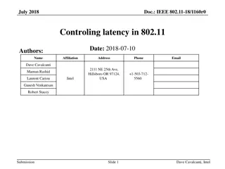
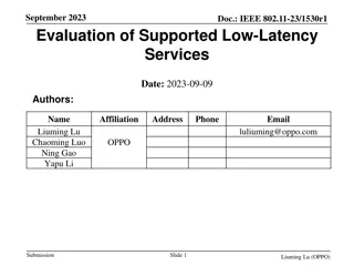
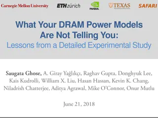
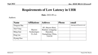
Understanding Latency Variation in Modern DRAM Chips Experimental Characterization, Analysis, and Optimization Kevin Chang Abhijith Kashyap, Hasan Hassan, Saugata Ghose, Kevin Hsieh, Donghyuk Lee, Tianshi Li, Gennady Pekhimenko,Samira Khan, Onur Mutlu v1.3
Main Memory Latency Lags Behind Capacity Bandwidth Latency64x 100 Improvement 16x 10 1.2x 1 1999 2003 2006 2008 2011 2013 2014 2015 Long DRAM latency performance bottleneck In-memory DB, Spark, JVM, [Clapp+ (Intel), IISWC 15] Google warehouse-scale workloads [Kanev+ (Google), ISCA 15] 2
Why is Latency High? DRAM latency: Delay as specified in DRAM standards Doesn t reflect true DRAM device latency Imperfect manufacturing process latency variation High standard latency chosen to increase yield DRAM A DRAM B DRAM C Standard Latency Manufacturing Variation High Low DRAM Latency 3
Goals 1 Understand and characterize latency variation in modern DRAM chips 1 2 Develop a mechanism that exploits latency variation to reduce DRAM latency 2 4
Outline Motivation and Goals DRAM Background Experimental Methodology Characterization Results Mechanism: Flexible-Latency DRAM Conclusion 5
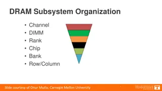
High-Level DRAM Organization DRAM chip DRAM Channel DIMM (Dual in-line memory module) 6
DRAM Chip Internals DRAM Cell Row Buffer 8KB (128 cache lines) 7
DRAM Operations 1 ACTIVATE: Store the row into the row buffer 1 1 1 1 2 READ: Select the target cache line and drive to CPU 3 PRECHARGE: Prepare the array for a new ACTIVATE to CPU 8
DRAM Timing Parameters 1 Activation latency: tRCD (13ns / 50 cycles) 2 Precharge latency: tRP (13ns / 50 cycles) ACTIVATE READ PRECHARGE Command 1 1 1 1 Cache line (64B) Data Duration Next ACT 9
DRAM Latency Variation Imperfect manufacturing process latency variation DRAM A DRAM B DRAM C Slow cells Low High DRAM Latency 10
Experimental Questions Imperfect manufacturing process latency variation Can we show latency variation in these parameters? How large is latency variation in modern DRAM chips? Can we identify the properties of slow cells with long latency? Can we isolate slow cells to make DRAM faster? 11
Experimental Methodology Tool that enables us to freely issue DRAM commands Existing systems: Commands are generated and controlled by HW Custom FPGA-based infrastructure PCIe DDR3 PC DIMM FPGA Generate C++ programs to specify commands command sequence 12
Experiments Swept each timing parameter to read data Time step of 2.5ns (FPGA cycle time) Quantified timing errors: bit flips when using reduced latency Tested 240 DDR3 DRAM chips from three vendors 30 DIMMs Manufacturing dates: 2011 2013 Capacity: 1GB Ambient temperature: 20oC 13
Outline Motivation and Goals DRAM Background Experimental Methodology Characterization Results Activation latency Precharge latency Mechanism: Flexible-Latency DRAM Conclusion 14
Activation Latency: Key Observation Observation: ACT errors are isolated in the cells read in the first cache line 1 1 1 1 Not fully activated ? 1 1 1 ? Row Buffer Second read w/ sufficient activation time 0 1 tRCD X READ ACTIVATE Actual ACT Time READ Command 15
Variation in Activation Errors Results from 7500 rounds over 240 chips Max No ACT Errors Many errors Rife w/ errors Quartiles Very few errors Min 13.1ns standard Modern DRAM chips exhibit Different characteristics across DIMMs significant variation in activation latency 16
Spatial Locality of Activation Errors One DIMM @ tRCD=7.5ns Activation errors are concentrated at certain columns of cells 17
Strong Pattern Dependence DIMM A DIMM B DIMM C > 4 orders of magnitude Row buffer design is biased towards 1 over 0 [Lim+, ISSCC 12] Activation errors have a strong dependence on the stored data patterns 18
Precharge Latency: Key Observation Observation: PRE errors occur in multiple cache lines in the row activated after a precharge 1 0 1 0 1 0 1 0 Not fully precharged 1 1 0 1 1 0 Row Buffer Incorrectly sensed data tRP PRECHARGE Actual PRE Time ACTIVATE Command 19
Variation in Precharge Errors Results from 4000 rounds over 240 chips Many errors No PRE Errors Rife w/ errors Few errors 13.1ns standard Different characteristics across DIMMs Modern DRAM chips exhibit significant variation in precharge latency 20
Spatial Locality of Precharge Errors One DIMM @ tRP=7.5ns Precharge errors are concentrated at certain rows of cells 21
Outline Motivation and Goals DRAM Background Experimental Methodology Characterization Results Mechanism: Flexible-Latency DRAM Conclusion 22
Mechanism to Reduce DRAM Latency Observations DRAM timing errors are concentrated on certain regions All cells operate without errors at 10ns tRCD and tRP Flexible-LatencY (FLY) DRAM A software-transparent design that reduces latency Key idea: 1) Divide memory into regions of different latencies 2) Memory controller: Uselower latency for regions without slow cells; higher latency for other regions 23
FLY-DRAM Evaluation Methodology Cycle-level simulator: Ramulator [CAL 15] https://github.com/CMU-SAFARI/ramulator 8-core system with DDR3 memory Benchmarks: SPEC2006, TPC, STREAM, random 40 8-core workloads Performance metric: Weighted Speedup (WS) 24
FLY-DRAM Configurations 100% Fraction of Cells tRCD 80% 60% 13ns 10ns 7.5ns 99% 40% 93% 20% 12% 0% Baseline (DDR3) D1 Profiles of 3 real DIMMs D2 D3 Upper Bound 100% Fraction of Cells tRP 80% 60% 13ns 10ns 7.5ns 99% 40% 74% 20% 13% 0% Baseline (DDR3) D1 D2 D3 Upper Bound 25
Results 1.25 19.5%19.7% 1.2 Normalized Performance 17.6% 1.15 13.3% Baseline (DDR3) FLY-DRAM (D1) FLY-DRAM (D2) FLY-DRAM (D3) Upper Bound 1.1 1.05 1 0.95 FLY-DRAM improves performance by exploiting latency variation in DRAM 0.9 40 Workloads 26
Other Results in the Paper Error-correcting codes (ECC) Effective at correcting activation errors Restoration latency Significant margin to complete without errors Effect of temperature Difference is not statistically significant to draw conclusion 27
Conclusion First to experimentally demonstrate and analyze latency variation behavior within real DRAM chips Show across 240 DRAM chips that: All cells work below standard latency Some regions of cells work even faster, but slow cells in other regions start to fail Error rate is data-dependent FLY-DRAM reduces latency by using low latency for regions without slow cells and high latency for others 13%/17%/19% speedup based on profiles of 3 real DIMMs https://github.com/CMU-SAFARI/DRAM-Latency-Variation-Study 28
Understanding Latency Variation in Modern DRAM Chips Experimental Characterization, Analysis, and Optimization Kevin Chang Abhijith Kashyap, Hasan Hassan, Saugata Ghose, Kevin Hsieh, Donghyuk Lee, Tianshi Li, Gennady Pekhimenko, Samira Khan, Onur Mutlu
Infrastructure Temperature Controller FPGA DIMM Heater 31
DRAM DIMMs 32
Activation Latency Variation by DRAM Models 33
Precharge Latency Variation by DRAM Models 37