Insights into DRAM Power Consumption and Design Concerns

W
h
a
t
 
Y
o
u
r
 
D
R
A
M
 
P
o
w
e
r
 
M
o
d
e
l
s
A
r
e
 
N
o
t
 
T
e
l
l
i
n
g
 
Y
o
u
:
L
e
s
s
o
n
s
 
f
r
o
m
 
a
 
D
e
t
a
i
l
e
d
 
E
x
p
e
r
i
m
e
n
t
a
l
 
S
t
u
d
y
 
Saugata Ghose, 
A. Giray Yağlıkçı, Raghav Gupta, Donghyuk Lee,
Kais Kudrolli, William X. Liu, Hasan Hassan, Kevin K. Chang,
Niladrish Chatterjee, Aditya Agrawal, Mike O’Connor, Onur Mutlu
 
June 21, 2018
D
R
A
M
 
P
o
w
e
r
 
I
s
 
B
e
c
o
m
i
n
g
 
a
 
M
a
j
o
r
 
D
e
s
i
g
n
 
C
o
n
c
e
r
n
 
Main memory in computers
consists of DRAM modules
DRAM consumes 
up to half
of total system power
State-of-the-art DRAM power models are not adequate
Based on 
IDD values: 
standard current measurements provided by vendors
Often have a 
high mean absolute percentage error
»
32% for DRAMPower
»
161% for Micron power model
P
age 2 of 20
OUR GOAL
Measure and analyze the power used by real DRAM,
and build an accurate DRAM power model
Fraction of
Total System Energy
 
B
a
c
k
g
r
o
u
n
d
:
 
D
R
A
M
 
O
r
g
a
n
i
z
a
t
i
o
n
 
&
 
O
p
e
r
a
t
i
o
n
C
h
a
r
a
c
t
e
r
i
z
a
t
i
o
n
 
M
e
t
h
o
d
o
l
o
g
y
N
e
w
 
F
i
n
d
i
n
g
s
 
o
n
 
D
R
A
M
 
P
o
w
e
r
 
C
o
n
s
u
m
p
t
i
o
n
V
A
M
P
I
R
E
:
 
A
 
V
a
r
i
a
t
i
o
n
-
A
w
a
r
e
 
D
R
A
M
 
P
o
w
e
r
 
M
o
d
e
l
C
o
n
c
l
u
s
i
o
n
 
P
age 3 of 20
 
O
u
t
l
i
n
e
S
i
m
p
l
i
f
i
e
d
 
D
R
A
M
 
O
r
g
a
n
i
z
a
t
i
o
n
 
a
n
d
 
O
p
e
r
a
t
i
o
n
 
Fundamental DRAM commands: activate, read, write,
precharge
One row of DRAM: 8 kB
One cache line of data: 64 B
P
age 4 of 20
DRAM Chip
Bank 0
 
. . .
 
. . .
Processor Chip
Memory Controller
 
Column Select
 
Bank Select
I/O Drivers
I/O Drivers
 
memory channel
DRAM
Cell Array
Row Buffer
Bank 7
 
activation
Core
.
 
.
 
.
Core
Shared Last-Level Cache
 
B
a
c
k
g
r
o
u
n
d
:
 
D
R
A
M
 
O
r
g
a
n
i
z
a
t
i
o
n
 
&
 
O
p
e
r
a
t
i
o
n
C
h
a
r
a
c
t
e
r
i
z
a
t
i
o
n
 
M
e
t
h
o
d
o
l
o
g
y
N
e
w
 
F
i
n
d
i
n
g
s
 
o
n
 
D
R
A
M
 
P
o
w
e
r
 
C
o
n
s
u
m
p
t
i
o
n
V
A
M
P
I
R
E
:
 
A
 
V
a
r
i
a
t
i
o
n
-
A
w
a
r
e
 
D
R
A
M
 
P
o
w
e
r
 
M
o
d
e
l
C
o
n
c
l
u
s
i
o
n
 
P
age 5 of 20
 
O
u
t
l
i
n
e
P
age 6 of 20
M
e
t
h
o
d
o
l
o
g
y
 
D
e
t
a
i
l
s
 
SoftMC: an FPGA-based memory controller 
[Hassan+ HPCA ’17]
Modified to repeatedly loop commands
Open-source: 
https://github.com/CMU-SAFARI/SoftMC
 
Measure current consumed by a module during a SoftMC test
 
Tested 
50 DDR3L DRAM modules
 
(200 DRAM chips)
Supply voltage: 1.35 V
Three major vendors: A, B, C
Manufactured between 2014 and 2016
 
For each experimental test that we perform
10 runs of each test per module
At least 10 current samples per run
P
age 7 of 20
 
B
a
c
k
g
r
o
u
n
d
:
 
D
R
A
M
 
O
r
g
a
n
i
z
a
t
i
o
n
 
&
 
O
p
e
r
a
t
i
o
n
C
h
a
r
a
c
t
e
r
i
z
a
t
i
o
n
 
M
e
t
h
o
d
o
l
o
g
y
N
e
w
 
F
i
n
d
i
n
g
s
 
o
n
 
D
R
A
M
 
P
o
w
e
r
 
C
o
n
s
u
m
p
t
i
o
n
V
A
M
P
I
R
E
:
 
A
 
V
a
r
i
a
t
i
o
n
-
A
w
a
r
e
 
D
R
A
M
 
P
o
w
e
r
 
M
o
d
e
l
C
o
n
c
l
u
s
i
o
n
 
P
age 8 of 20
 
O
u
t
l
i
n
e
1
.
 
R
e
a
l
 
D
R
A
M
 
P
o
w
e
r
 
V
a
r
i
e
s
 
W
i
d
e
l
y
 
f
r
o
m
 
I
D
D
 
V
a
l
u
e
s
 
Different vendors have very different margins (i.e.,
guardbands
)
Low variance among different modules from same vendor
P
age 9 of 20
IDD2N
Idle
IDD0
Activate–Precharge
IDD4R
Read
Current consumed by real DRAM modules
varies significantly for all IDD values that we measure
2
.
 
D
R
A
M
 
P
o
w
e
r
 
i
s
 
D
e
p
e
n
d
e
n
t
 
o
n
 
D
a
t
a
 
V
a
l
u
e
s
 
Some variation due to infrastructure – can be subtracted
Without infrastructure variation: up to 230 mA of change
Toggle affects power consumption, but < 0.15 mA per bit
Page 10 of 20
DRAM power consumption depends 
strongly
on the data value, but not on bit toggling
3
.
 
S
t
r
u
c
t
u
r
a
l
 
V
a
r
i
a
t
i
o
n
 
A
f
f
e
c
t
s
 
D
R
A
M
 
P
o
w
e
r
 
U
s
a
g
e
 
Vendor C: variation in
idle current across
banks
 
All vendors: variation in
read current across
banks
 
All vendors: variation in
activation based on
row address
Page 11 of 20
Significant structural variation:
DRAM power varies systematically by bank and row
4
.
 
G
e
n
e
r
a
t
i
o
n
a
l
 
S
a
v
i
n
g
s
 
A
r
e
 
S
m
a
l
l
e
r
 
T
h
a
n
 
E
x
p
e
c
t
e
d
 
Similar trends for idle and read currents
Page 12 of 20
IDD0
Activate–Precharge
IDD4W
Write
Actual power savings of newer DRAM is 
much lower
than the savings indicated in the datasheets
 
S
u
m
m
a
r
y
 
o
f
 
N
e
w
 
O
b
s
e
r
v
a
t
i
o
n
s
 
o
n
 
D
R
A
M
 
P
o
w
e
r
 
1.
Real DRAM modules often 
consume less power
than vendor-provided IDD values state
 
2.
DRAM power consumption is 
dependent on the data value
that is read/written
 
3.
Across banks and rows, 
structural variation affects power
consumption of DRAM
 
4.
Newer DRAM modules save less power
 than indicated in
datasheets by vendors
 
Detailed observations and analyses in the paper
 
Page 13 of 20
 
B
a
c
k
g
r
o
u
n
d
:
 
D
R
A
M
 
O
r
g
a
n
i
z
a
t
i
o
n
 
&
 
O
p
e
r
a
t
i
o
n
C
h
a
r
a
c
t
e
r
i
z
a
t
i
o
n
 
M
e
t
h
o
d
o
l
o
g
y
N
e
w
 
F
i
n
d
i
n
g
s
 
o
n
 
D
R
A
M
 
P
o
w
e
r
 
C
o
n
s
u
m
p
t
i
o
n
V
A
M
P
I
R
E
:
 
A
 
V
a
r
i
a
t
i
o
n
-
A
w
a
r
e
 
D
R
A
M
 
P
o
w
e
r
 
M
o
d
e
l
C
o
n
c
l
u
s
i
o
n
 
Page 14 of 20
 
O
u
t
l
i
n
e
A
 
N
e
w
 
V
a
r
i
a
t
i
o
n
-
A
w
a
r
e
 
D
R
A
M
 
P
o
w
e
r
 
M
o
d
e
l
 
VAMPIRE: Variation-Aware model of Memory Power
Informed by Real Experiments


VAMPIRE and raw characterization data will be open-source:
https://github.com/CMU-SAFARI/VAMPIRE
 (August 2018)
Page 15 of 20
VAMPIRE
Read/Write and
Data-Dependent
Power Modeling
Idle/Activate/Precharge
Power Modeling
Structural Variation Aware
Power Modeling
 
Inputs
(from memory system
simulator)
Trace of DRAM
commands, timing
Data
 that is
being written
 
Outputs
Per-vendor
power
consumption
Range for
each
 vendor
(optional)
V
A
M
P
I
R
E
 
H
a
s
 
L
o
w
e
r
 
E
r
r
o
r
 
T
h
a
n
 
E
x
i
s
t
i
n
g
 
M
o
d
e
l
s
Validated using new power measurements: details in the paper
Page 16 of 20
VAMPIRE has very low error for 
all
 vendors: 6.8%
Much more accurate than prior models
 
V
A
M
P
I
R
E
 
E
n
a
b
l
e
s
 
S
e
v
e
r
a
l
 
N
e
w
 
S
t
u
d
i
e
s
 
Taking advantage of structural variation to perform
variation-aware physical page allocation
 to reduce power
 
Smarter DRAM 
power-down scheduling
 
Reducing DRAM energy with 
data-dependency-aware
cache line encodings
23 applications from
the SPEC 2006
benchmark suite
Traces collected using
Pin and Ramulator
 
We expect there to be many other new studies in the future
 
Page 17 of 20
 
B
a
c
k
g
r
o
u
n
d
:
 
D
R
A
M
 
O
r
g
a
n
i
z
a
t
i
o
n
 
&
 
O
p
e
r
a
t
i
o
n
C
h
a
r
a
c
t
e
r
i
z
a
t
i
o
n
 
M
e
t
h
o
d
o
l
o
g
y
N
e
w
 
F
i
n
d
i
n
g
s
 
o
n
 
D
R
A
M
 
P
o
w
e
r
 
C
o
n
s
u
m
p
t
i
o
n
V
A
M
P
I
R
E
:
 
A
 
V
a
r
i
a
t
i
o
n
-
A
w
a
r
e
 
D
R
A
M
 
P
o
w
e
r
 
M
o
d
e
l
C
o
n
c
l
u
s
i
o
n
 
Page 18 of 20
 
O
u
t
l
i
n
e
C
o
n
c
l
u
s
i
o
n
 
DRAM consumes 
up to half of total system power
:
need to develop new low-power solutions
State-of-the-art DRAM power models are based only on
IDD values, and 
have a high error
We make 
four new observations
 on DRAM power
consumption using 50 real DRAM modules from three major
vendors
Real DRAM modules often 
consume less power
 than IDD values state
Power consumption is 
dependent on the data value
 being read/written
Across banks and rows, 
structural variation affects power
 consumption
Newer DRAM modules save less power
 than indicated in datasheets
VAMPIRE:
 
a new DRAM power model built on our
observations
Mean absolute percentage 
error of only 6.8%
Case study: dependency-aware data encoding 
reduces DRAM power by
12%
Page 19 of 20
More information: 
https://github.com/CMU-SAFARI/VAMPIRE
W
h
a
t
 
Y
o
u
r
 
D
R
A
M
 
P
o
w
e
r
 
M
o
d
e
l
s
A
r
e
 
N
o
t
 
T
e
l
l
i
n
g
 
Y
o
u
:
L
e
s
s
o
n
s
 
f
r
o
m
 
a
 
D
e
t
a
i
l
e
d
 
E
x
p
e
r
i
m
e
n
t
a
l
 
S
t
u
d
y
 
Saugata Ghose, 
A. Giray Yağlıkçı, Raghav Gupta, Donghyuk Lee,
Kais Kudrolli, William X. Liu, Hasan Hassan, Kevin K. Chang,
Niladrish Chatterjee, Aditya Agrawal, Mike O’Connor, Onur Mutlu
 
More information: 
https://github.com/CMU-SAFARI/VAMPIRE
 
Backup Slides
 
 
Page 21 of 20
 
M
o
r
e
 
I
n
f
o
r
m
a
t
i
o
n
 
i
n
 
t
h
e
 
P
a
p
e
r
 
Full characterization analysis
 
Application-level comparison to existing power models
 
Case study: dependency-aware data encoding


Paper available at 
https://github.com/CMU-
SAFARI/VAMPIRE
 
Page 22 of 20
T
o
d
a
y
s
 
M
o
d
e
l
s
 
L
e
a
v
e
 
a
 
L
o
t
 
t
o
 
B
e
 
D
e
s
i
r
e
d
 
Most models reliant on JEDEC-based IDD values
Micron power calculator
DRAMPower
gem5/GPGPU-Sim
 
Some rely on circuit-level models
Vogelsang model for memory scaling
CACTI
 
None are all that accurate
One value for each DRAM
Does not capture any inherent variation (e.g., data, structure)
Page 23 of 20
H
o
w
 
D
o
 
W
e
 
M
e
a
s
u
r
e
 
C
u
r
r
e
n
t
?
 
Page 24 of 20
Cmd Buffer
Hassan et al. “SoftMC:  A Flexible and Practical Open-Source Infrastructure 
for Enabling Experimental DRAM Studies,” HPCA, 2017.
[1]
 
F
o
u
n
d
a
t
i
o
n
 
o
f
 
C
u
r
r
e
n
t
 
P
o
w
e
r
 
M
o
d
e
l
s
 
Just how bad are current models?
 
JEDEC defines a set of IDD values
 
Page 25 of 20
W
h
a
t
s
 
S
o
 
B
a
d
 
A
b
o
u
t
 
T
h
a
t
?
 
JEDEC defined IDD measurement loops cover:
Average power consumption of all banks
»
missing variation across banks
Average power consumption of only two rows: 00 and F0
»
missing variation across rows in a subarray
»
missing variation across subarrays
Average power consumption of only two data patterns: 00 and 33
»
missing effect of number of ones/zeros in data
»
missing effect of toggling bits
Page 26 of 20
 
I
D
D
0
:
 
A
c
t
i
v
a
t
i
o
n
 
a
n
d
 
P
r
e
c
h
a
r
g
e
 
E
n
e
r
g
y
 
Page 27 of 20
DRAM Array


Row Buffer
 
0x00
 
0xF0
 
I
D
D
1
:
 
A
c
t
i
v
a
t
i
o
n
,
 
R
e
a
d
,
 
a
n
d
 
P
r
e
c
h
a
r
g
e
 
E
n
e
r
g
y
 
Page 28 of 20
Row Buffer
 
I
D
D
2
N
:
 
P
r
e
c
h
a
r
g
e
d
 
S
t
a
n
d
b
y
 
Page 29 of 20
 
Bank 0
 
Bank 1
 
Bank 7
 
(1) Precharge All Banks
     (Close Row Buffers)
 
(2) Wait
 
I
D
D
3
N
:
 
A
c
t
i
v
e
 
S
t
a
n
d
b
y
 
Page 30 of 20
 
Bank 0
 
Bank 1
 
Bank 7
 
(1)
Activate All Banks
     (Open Row Buffers)
 
(2) Wait
 
I
D
D
2
P
:
 
P
r
e
c
h
a
r
g
e
d
 
P
o
w
e
r
 
D
o
w
n
 
Page 31 of 20
 
Bank 0
 
Bank 1
 
Bank 7
 
(1) Precharge All Banks
     (Close Row Buffers)
 
(2) Wait
CLK is Disabled
 
I
D
D
4
R
:
 
B
u
r
s
t
 
R
e
a
d
 
C
u
r
r
e
n
t
 
Page 32 of 20
 
Bank 0
 
Bank 1
 
Bank 7
 
(1)
Activate All Banks
     (Open Row Buffers)
 
(2) Read one column
      at a time
 
(3) Interleave across
     banks after each read
 
I
D
D
4
W
:
 
B
u
r
s
t
 
W
r
i
t
e
 
C
u
r
r
e
n
t
 
Page 33 of 20
 
Bank 0
 
Bank 1
 
Bank 7
 
(1)
Activate All Banks
     (Open Row Buffers)
 
(2) Write one column
      at a time
 
(3) Interleave across
     banks after each read
 
I
D
D
5
B
:
 
R
e
f
r
e
s
h
 
i
n
 
B
u
r
s
t
 
M
o
d
e
 
Page 34 of 20
 
t
R
E
F
I
(
6
4
m
s
)
 
B
u
r
s
t
 
M
o
d
e
:
 
REF
 
t
RFC
 
A
C
T
-
R
D
A
 
I
D
D
7
:
 
R
e
a
d
,
 
A
u
t
o
-
P
r
e
c
h
a
r
g
e
 
Page 35 of 20
 
t
RRD
 
A
C
T
-
R
D
A
 
t
RRD
 
I
m
p
a
c
t
 
o
f
 
B
i
t
 
T
o
g
g
l
i
n
g
 
o
n
 
D
R
A
M
 
P
o
w
e
r
 
Page 36 of 20
0000  1010  1111  …  0011
 
Bank 0 Row Buffer
 
0
 
1
 
column
number
 
2
 
c 
– 1
1011  0010  1011  …  0110
 
Bank 1 Row Buffer
 
0
 
1
 
2
 
c 
– 1
1011  0010  1011  …  0110
 
Bank 7 Row Buffer
 
0
 
1
 
2
 
c 
– 1
1
2
 
. . .
 
. . .
 
. . .
 
. . .
 
. . .
 
. . .
 
. . .
 
Column Select
 
Column Select
 
Column Select
 
Bank Select
 
global bitlines
 
peripheral bus
to I/O drivers
 
global bitlines
 
D
a
t
a
 
D
e
p
e
n
d
e
n
c
y
 
M
o
d
e
l
 
Page 37 of 20
y = F + Gn + Ht
 
Additional current per bit toggle
 
Additional current per logic-1
 
M
o
d
e
l
s
 
Page 38 of 20
 
https://github.com/CMU-SAFARI/VAMPIRE
S
t
r
u
c
t
u
r
a
l
 
V
a
r
i
a
t
i
o
n
Page 39 of 20
 
E
v
a
l
u
a
t
e
d
 
S
y
s
t
e
m
 
C
o
n
f
i
g
u
r
a
t
i
o
n
 
Application traces collected using Pin
 
DRAM command timings generated using Ramulator:
https://github.com/CMU-SAFARI/ramulator
 
Page 40 of 20
 
T
r
e
n
d
s
 
A
c
r
o
s
s
 
G
e
n
e
r
a
t
i
o
n
s
 
Basically, if
you’re building
a system, you
aren’t getting
the kinds of
savings you
were promised
 
Page 41 of 20
 
Activation Energy
 
Precharge Standby Energy
 
Read Energy
 
Write Energy
 
D
a
t
a
 
E
n
c
o
d
i
n
g
 
Baseline: No coding
BDI: Base Delta Immediate
Optimized: Minimize the number of ones
OWI: Minimize ones for reads, maximize ones for writes
 
Page 42 of 20
 
12.5%
Energy
Reduction
 
V
a
l
i
d
a
t
i
n
g
 
O
u
r
 
D
R
A
M
 
P
o
w
e
r
 
M
o
d
e
l
s
 
New tests run on 22 of our DDR3L DRAM SO-DIMMs
Validation command sequence
Activate
n
 reads
»
Sweep 
n
 from 0 to 764
»
All reads contain data value 0xAA
»
All reads to Bank 0, Row 128
»
Column interleaved
Precharge
Error metric: mean absolute percentage error (MAPE)
 
Best prior model (DRAMPower): 32.4% MAPE
VAMPIRE: 6.8% MAPE
 
Page 43 of 20
Slide Note
Embed
Share

Detailed experimental study reveals that DRAM power models may not provide accurate insights into power consumption. The increasing importance of managing DRAM power in system design is emphasized. The study delves into DRAM organization, operation, and power consumption patterns, highlighting the need for a variation-aware DRAM power model for more precise calculations.

  • DRAM power
  • System energy
  • Design concerns
  • Power consumption
  • Experimental study

Uploaded on Aug 13, 2024 | 0 Views


Download Presentation

Please find below an Image/Link to download the presentation.

The content on the website is provided AS IS for your information and personal use only. It may not be sold, licensed, or shared on other websites without obtaining consent from the author. Download presentation by click this link. If you encounter any issues during the download, it is possible that the publisher has removed the file from their server.

E N D

Presentation Transcript


  1. What Your DRAM Power Models Are Not Telling You: Lessons from a Detailed Experimental Study

  2. DRAM Power Is Becoming a Major Design Concern 0.5 Total System Energy 0.4 0.3 Fraction of 0.2 0.1 0.0 Malladi+ ISCA '12 ISCA '15 Report '16 HPCA '10 ICAC '11 ISCA '12 David+ Elmore+ Ware+ Paul+ Yoon Page 2 of 20

  3. Outline Background: DRAM Organization & Operation Characterization Methodology New Findings on DRAM Power Consumption VAMPIRE: A Variation-Aware DRAM Power Model Conclusion Page 3 of 20

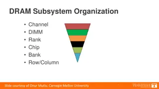
  4. Simplified DRAM Organization and Operation DRAM Chip . . . Bank 0 Bank 7 Processor Chip DRAM Cell Array . . . activation Core Core Row Buffer Column Select Shared Last-Level Cache . . . Memory Controller Bank Select I/O Drivers I/O Drivers memory channel Page 4 of 20

  5. Outline Background: DRAM Organization & Operation Characterization Methodology New Findings on DRAM Power Consumption VAMPIRE: A Variation-Aware DRAM Power Model Conclusion Page 5 of 20

  6. Power Measurement Platform Keysight 34134A DC Current Probe DDR3L SO-DIMM Virtex 6 FPGA JET-5467A Riser Board Page 6 of 20

  7. Methodology Details Page 7 of 20

  8. Outline Background: DRAM Organization & Operation Characterization Methodology New Findings on DRAM Power Consumption VAMPIRE: A Variation-Aware DRAM Power Model Conclusion Page 8 of 20

  9. 1. Real DRAM Power Varies Widely from IDD Values 100 200 800 Datasheet Corrected Datasheet Measured 80 Current (mA) Current (mA) 150 600 Current (mA) 60 100 400 40 50 200 20 0 0 0 A B C A B C A B C Page 9 of 20

  10. 2. DRAM Power is Dependent on Data Values 800 800 Write Current (mA) Read Current (mA) Vendor A Vendor B Vendor C 600 600 400 400 Vendor A Vendor B Vendor C 200 200 0 0 0 Number of Ones in a Cache Line 128 256 384 512 0 Number of Ones in a Cache Line 128 256 384 512 Page 10 of 20

  11. 3. Structural Variation Affects DRAM Power Usage 1.4 Idle Current Normalized 1.2 1.0 0.8 0 1 2 3 4 5 6 7 0 1 2 3 4 5 6 7 0 1 2 3 4 5 6 7 Vendor A Vendor B Vendor C 1.1 Read Current Normalized 1.0 0.9 0.8 0 1 2 3 4 5 6 7 0 1 2 3 4 5 6 7 0 1 2 3 4 5 6 7 Vendor A Vendor B Vendor C 1.20 1.15 1.10 1.05 1.00 0.95 Normalized Measured Vendor A Vendor B Vendor C Current 0 1 2 3 4 5 6 7 8 9 10 11 12 13 14 15 Number of Ones in Row Address Page 11 of 20

  12. 4. Generational Savings Are Smaller Than Expected Page 12 of 20

  13. Summary of New Observations on DRAM Power Page 13 of 20

  14. Outline Background: DRAM Organization & Operation Characterization Methodology New Findings on DRAM Power Consumption VAMPIRE: A Variation-Aware DRAM Power Model Conclusion Page 14 of 20

  15. A New Variation-Aware DRAM Power Model Inputs VAMPIRE Outputs (from memory system simulator) Read/Write and Data-Dependent Power Modeling Per-vendor power consumption Trace of DRAM commands, timing Idle/Activate/Precharge Power Modeling Range for each vendor (optional) Data that is being written Structural Variation Aware Power Modeling Page 15 of 20

  16. VAMPIRE Has Lower Error Than Existing Models 250% Micron Model DRAMPower VAMPIRE Percentage Error Mean Absolute 200% 160.6% 150% 100% 50% 32.4% 6.8% 0% Vendor A (8 modules) Vendor B (7 modules) Vendor C (7 modules) GMean Page 16 of 20

  17. VAMPIRE Enables Several New Studies 1.2 Baseline BDI Optimized OWI DRAM Energy Normalized 1.1 -12.2% 1.0 0.9 0.8 0.7 Vendor A Vendor B Vendor C GMean Page 17 of 20

  18. Outline Background: DRAM Organization & Operation Characterization Methodology New Findings on DRAM Power Consumption VAMPIRE: A Variation-Aware DRAM Power Model Conclusion Page 18 of 20

  19. Conclusion Page 19 of 20

  20. What Your DRAM Power Models Are Not Telling You: Lessons from a Detailed Experimental Study

  21. Backup Slides Page 21 of 20

  22. More Information in the Paper 1.1 Normalized Baseline BDI Optimized OWI Energy 1.0 0.9 0.8 Vendor A Vendor B Vendor C Page 22 of 20

  23. Todays Models Leave a Lot to Be Desired Page 23 of 20

  24. How Do We Measure Current? VDD USB Host PC Probe PCI-e FPGA DRAM Module PCI-e IF Cmd Buffer Rank . . . Chip Chip memory channel SoftMC [1] [1] Hassan et al. SoftMC: A Flexible and Practical Open-Source Infrastructure for Enabling Experimental DRAM Studies, HPCA, 2017. Page 24 of 20

  25. Foundation of Current Power Models IDD0 Activation and Precharge IDD1 Activation 1 Column Read Precharge IDD2N Precharge Standby (all banks are precharged/closed) clk enabled IDD3N Active Standby (all banks are active/opened) clk enabled IDD2P Precharge Power-Down (all banks are precharged/closed) clk disabled IDD3P Active Power-Down (all banks are active/opened) clk disabled IDD4R/W Burst mode Read/Write IDD5B Burst mode Refresh IDD7 Activate Column Read w/ Auto Precharge Page 25 of 20

  26. Whats So Bad About That? Page 26 of 20

  27. IDD0: Activation and Precharge Energy DRAM Array tRAS tRP tRAS 0xF0 ACT PRE ACT PRE time 0x00 Row Buffer Measured Current0.50 0.30 200 Datasheet Measured 0.45 150 Normalized Current (mA) 0.40 100 0.35 50 0 A B C Vendor A Vendor B Vendor C Page 27 of 20

  28. IDD1: Activation, Read, and Precharge Energy DRAM Array 0xF0 tRCD tRP PRE RD ACT ACT tRAS 0x00 time Row Buffer Measured Current0.70 0.20 350 Datasheet Measured 300 0.60 Current (mA) Normalized 250 0.50 200 150 0.40 100 0.30 50 0 Vendor A Vendor B Vendor C A B C Page 28 of 20

  29. IDD2N: Precharged Standby Bank 0 Bank 1 DRAM Array Bank 7 DRAM Array DRAM Array (1) Precharge All Banks (Close Row Buffers) (2) Wait Row Buffer Row Buffer Row Buffer Measured Current1.00 0.20 0.80 Normalized 0.60 0.40 A B C Page 29 of 20

  30. IDD3N: Active Standby Bank 0 Bank 1 Bank 7 DRAM Array DRAM Array DRAM Array (1) Activate All Banks (Open Row Buffers) (2) Wait Row Buffer Row Buffer Row Buffer Measured Current0.70 0.20 0.10 200 Datasheet Measured 0.60 150 Current (mA) Normalized 0.50 100 0.40 0.30 50 0 Vendor A Vendor B Vendor C A B Page 30 of 20 C

  31. IDD2P: Precharged Power Down Bank 0 Bank 1 DRAM Array Bank 7 DRAM Array DRAM Array (1) Precharge All Banks (Close Row Buffers) (2) Wait Row Buffer Row Buffer Row Buffer Measured Current1.20 0.20 0.00 80 Datasheet Measured 1.00 60 Current (mA) Normalized 0.80 40 0.60 0.40 20 0 Vendor A Vendor B Vendor C A B C Page 31 of 20

  32. IDD4R: Burst Read Current Bank 0 Bank 1 Bank 7 (1) Activate All Banks (Open Row Buffers) DRAM Array DRAM Array DRAM Array (2) Read one column at a time Row Buffer Row Buffer 15 0x00 0x33 Row Buffer 9 0x00 0x33 (3) Interleave across banks after each read 7 0 1 8 0x00 0x33 800 Datasheet Measured Corrected 600 Current (mA) 400 200 0 Vendor A Vendor B Vendor C Page 32 of 20

  33. IDD4W: Burst Write Current Bank 0 Bank 1 Bank 7 (1) Activate All Banks (Open Row Buffers) DRAM Array DRAM Array DRAM Array (2) Write one column at a time Row Buffer Row Buffer 15 0x00 0x33 Row Buffer 9 0x00 0x33 (3) Interleave across banks after each read 7 0 1 8 0x00 0x33 600 Datasheet Measured Current (mA) 400 200 0 Vendor A Vendor B Vendor C Page 33 of 20

  34. IDD5B: Refresh in Burst Mode Burst Mode: tRFC tRFC tREFI (64ms) REF REF REF time tRFC Measured Current1.00 0.50 0.90 Normalized 0.80 0.70 0.60 A B C Page 34 of 20

  35. IDD7: Read, Auto-Precharge ACT-RDA tRRD ACT-RDA tRRD ACT-RDA tRRD time 800 Measured Current0.65 0.35 Datasheet Measured 0.60 600 Current (mA) Normalized 0.55 400 0.50 0.45 200 0.40 0 A B C Vendor A Vendor B Vendor C Page 35 of 20

  36. Impact of Bit Toggling on DRAM Power . . . Bank 0 Row Buffer 1 Bank 1 Row Buffer 1 Bank 7 Row Buffer 1 column number 0 2 c 1 0 2 c 1 0 2 c 1 . . . 0000 1010 1111 0011 1011 0010 1011 0110 1011 0010 1011 0110 . . . . . . . . . . . . Column Select Column Select Column Select 1 . . . global bitlines global bitlines Bank Select 2 peripheral bus to I/O drivers Page 36 of 20

  37. Data Dependency Model Read Write F (mA) G (mA) H (mA) F (mA) G (mA) H (mA) Vendor A 246.44 0.433 0.0515 531.18 -0.246 0.0461 Vendor B 217.42 0.157 0.0947 466.84 -0.215 0.0166 Vendor C 234.42 0.154 0.0856 368.29 -0.116 0.0229 y = F + y = F + Gn Gn + + Ht Ht Additional current per logic-1 Additional current per bit toggle 800 800 Read Current (mA) Write Current (mA) 600 600 400 400 Vendor A Vendor B Vendor C 200 200 0 0 0 Number of Ones in a Cache Line 128 256 384 512 0 128 256 384 512 Number of Ones in a Cache Line Page 37 of 20

  38. Models https://github.com/CMU-SAFARI/VAMPIRE Page 38 of 20

  39. Structural Variation 1.4 Normalized Normalized Active Standby Active Standby Energy across Banks Current 1.2 1.0 0.8 0 12 3 4 5 6 7 0 12 3 4 5 6 7 0 12 3 4 5 6 7 Vendor A Vendor B Vendor C 1.1 Normalized Normalized Read Read Burst Energy across Banks Current 1.0 0.9 0.8 0 12 3 4 5 6 7 0 12 3 4 5 6 7 0 12 3 4 5 6 7 Vendor A Vendor B Vendor C 1.1 Write Current Normalized 1.0 0.9 Normalized Write Burst Write Burst Energy across Banks 0.8 0 12 3 4 5 6 7 0 12 3 4 5 6 7 0 12 3 4 5 6 7 Vendor A Vendor B Vendor C Page 39 of 20

  40. Evaluated System Configuration Processor x86-64 ISA, one core 3.2 GHz, 128-entry instruction window Cache L1: 64 kB, 4-way associative; L2: 2 MB, 16-way associative Memory Controller 64/64-entry read/write request queues, FR-FCFS [119, 149] DRAM DDR3L-800 [57], 1 channel, 1 rank/8 banks per channel Page 40 of 20

  41. Trends Across Generations 400 200 Datasheet Measured Datasheet Measured Current (mA) Current (mA) 300 150 -112.1mA -192.1mA 200 100 100 50 -53.7mA -64.0mA 0 0 2010 2011 2012 2013 2014 2015 Year Manufactured Activation Energy 2010 2011 2012 2013 2014 2015 Year Manufactured Precharge Standby Energy 700 700 Datasheet Measured Datasheet Measured 600 600 Current (mA) Current (mA) 500 500 -200.2mA -212.2mA -140.6mA 400 400 300 300 -147.4mA 200 200 100 100 0 0 2010 2011 2012 2013 2014 2015 Year Manufactured Read Energy 2010 2011 2012 2013 2014 2015 Year Manufactured Write Energy Page 41 of 20

  42. Data Encoding 1.2 Baseline BDI Optimized OWI Normalized Energy 12.5% Energy Reduction 1.0 0.8 0.6 Vendor A Vendor B Vendor C Page 42 of 20

  43. Validating Our DRAM Power Models Page 43 of 20

Related


More Related Content

giItT1WQy@!-/#giItT1WQy@!-/#giItT1WQy@!-/#giItT1WQy@!-/#giItT1WQy@!-/#giItT1WQy@!-/#giItT1WQy@!-/#giItT1WQy@!-/#giItT1WQy@!-/#giItT1WQy@!-/#giItT1WQy@!-/#giItT1WQy@!-/#giItT1WQy@!-/#giItT1WQy@!-/#giItT1WQy@!-/#giItT1WQy@!-/#giItT1WQy@!-/#giItT1WQy@!-/#giItT1WQy@!-/#giItT1WQy@!-/#