Understanding Diodes in Electronic Circuits
Learn about clamping networks, zener diodes, and how to analyze and utilize them in electronic circuits for signal clamping, voltage reference, and protection. Explore step-by-step procedures and examples to enhance your understanding.

Download Presentation

Please find below an Image/Link to download the presentation.
The content on the website is provided AS IS for your information and personal use only. It may not be sold, licensed, or shared on other websites without obtaining consent from the author. If you encounter any issues during the download, it is possible that the publisher has removed the file from their server.
You are allowed to download the files provided on this website for personal or commercial use, subject to the condition that they are used lawfully. All files are the property of their respective owners.
The content on the website is provided AS IS for your information and personal use only. It may not be sold, licensed, or shared on other websites without obtaining consent from the author.
E N D
Presentation Transcript
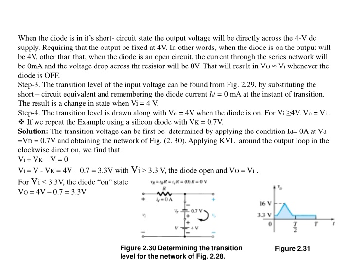
When the diode is in its short- circuit state the output voltage will be directly across the 4-V dc supply. Requiring that the output be fixed at 4V. In other words, when the diode is on the output will be 4V, other than that, when the diode is an open circuit, the current through the series network will be 0mA and the voltage drop across thr resistor will be 0V. That will result in VO Vi whenever the diode is OFF. Step-3. The transition level of the input voltage can be found from Fig. 2.29, by substituting the short circuit equivalent and remembering the diode current Id = 0 mA at the instant of transition. The result is a change in state when Vi = 4 V. Step-4. The transition level is drawn along with Vo = 4V when the diode is on. For Vi 4V. Vo = Vi . If we repeat the Example using a silicon diode with VK = 0.7V. Solution: The transition voltage can be first be determined by applying the condition Id= 0A at Vd =VD = 0.7V and obtaining the network of Fig. (2. 30). Applying KVL around the output loop in the clockwise direction, we find that : Vi + VK V = 0 Vi = V - VK = 4V 0.7 = 3.3V with Vi 3.3 V, the diode open and VO = Vi . For Vi 3.3V, the diode on state VO = 4V 0.7 = 3.3V Figure 2.30 Determining the transition level for the network of Fig. 2.28. Figure 2.31
2.9 CLAMPERS: The clamping network is one that will clamp a signal to a different dc level. The network must have a capacitor, a diode, and a resistive element. But it can also employ an independent dc supply to introduce an additional shift. The magnitude of R and C must be chosen such that the time constant RC is large enough to ensure that the voltage across the capacitor does not discharge significantly during the interval the diode is nonconducting. Throughout the analysis we will assume that for all practical purposes the capacitor will fully charge or discharge in five time constants. Figure 2.32 Clamper. The simplest of clamper network is provided in Fig.(2.32) . It is important to note that the capacitor is connected directly between input and output signals and the resistor and the diode are connected in parallel with the output signal.
In general, the following steps may be helpful when analyzing clamping networks: Step-1.Start the analysis of clamping networks by considering that part of the input signal that will forward bias the diode. Step-2. During the period that the diode is in the on state, assume that the capacitor will charge up instantaneously to a voltage level determined by the network. Step-3. Assume that during the period when the diode is in the off state the capacitor will hold on to its established voltage level. Step-4. Throughout the analysis maintain a continual awareness of the location and reference polarity for Vo to ensure that the proper levels for vo are obtained. Step-5. Keep in mind the general rule that the total swing of the total output must match the swing of the input signal. Example: Determine vo for the network of Fig. 2.36 for the input indicated.? Figure 2.36 Applied signal and network for Example
ID 2.10 ZENER DIODES Fig(2.37) reviews the approximate circuits for each region of a zener diode assuming the straight line approximations of each break. So how demonstrate a zener diode can be used to establish reference voltage levels and act as a protection device. The use of a zener diode as regulator will then be described to detail because it is one of its major areas of application. Aregulatr is a combination of elements designed to ensure that the output voltage of a supply remains fairly constant. VD Fig.(2. 37) Approximate equivalent circuits for the zener diode in the three possible regions of applications Example: Determine the reference voltages provided by the network of fig. (2.38) which uses a white LED (4V) to indicate power is on. What is the power delivered to the LED and to the 6 V Zener diode. Fig.(2.38) Reference setting circuit
Zener diode as a regulator: The basic configuration appears in fig. (2.39). The analysis is first for fixed quantities followed by a fixed supply voltage and a variable load, and finally a fixed load and avariable supply. Figure 2.39 Basic Zener regulator VI and RL fixed: The applied dc voltage is fixed, as is the load resistor. The analysis can be broken into two steps: 1. Determine the state of the Zener diode by removing it from the network and calculating the voltage across the resulting open circuit. (2 14) If V VZ, the Zener diode is on Figure 2.40 Determining the state of the Zener diode. If V VZ, the diode is off