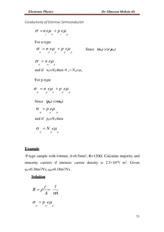
Introduction to Uni-Junction Transistor (UJT) in Electronic Semiconductors
Uni-Junction Transistor (UJT) is a semiconductor switching device with unique characteristics, such as regenerative emitter current increase when triggered, leading to a negative resistance region. It finds applications in sawtooth and pulse generation, switching, and triggering SCRs & TRIACs. The UJT symbol, equivalent circuit, construction, and working principles are discussed in detail.

Download Presentation

Please find below an Image/Link to download the presentation.
The content on the website is provided AS IS for your information and personal use only. It may not be sold, licensed, or shared on other websites without obtaining consent from the author.If you encounter any issues during the download, it is possible that the publisher has removed the file from their server.
You are allowed to download the files provided on this website for personal or commercial use, subject to the condition that they are used lawfully. All files are the property of their respective owners.
The content on the website is provided AS IS for your information and personal use only. It may not be sold, licensed, or shared on other websites without obtaining consent from the author.
E N D
Presentation Transcript
B.Sc.Sem-II Paper-I/Unit-II Uni-Junction Transistor(UJT) Introduction 1)A uni-junction transistor is an electronic semiconductor switching device that has only one junction and three terminals. 2)It has a unique characteristics that is whenever it is triggered ,its emitter current increases regeneratively while the corresponding voltage across it decreases .This property is called as Negative resistance region. 3)It is commonly used as saw tooth generator, pulse generator, switching and to trigger SCRs& TRIACs
Symbol of UJT 1) The symbol of UJT is different from the symbol of JFET 2) There is a tilt in the arrow by a small angle. 3) The symbolic representation of UJT is as shown fig1 4) The arrow on the emitter terminal indicates the direction of conventional current flow.
Equivalent circuit of UJT 1)Fig.2 shows the equivalent circuit diagram of UJT 2)It consist of two resistors RB1 and RB2,and a single diode D 3)RB1 is a variable resistor and RB2 is fixed resistor. 4)RB1 varies from 5k to 50 with IE 5)From fig2 i) RBB=RB1+RB2 ii) VRB1 =(RB1/RB1+RB2)*VBB = *VBB where is the intrinsic stand off ratio and it is in the range of 0.51 to 0.82 iii) VP = *VBB+VD Where VP is the peak point voltage at which UJT start conducting (fired)
Construction of UJT 1)Fig 3 shows constructional diagram of UJT 2)It consist of a lightly doped n-type silicon semiconductor bar provided with ohmic contacts on either side 3)The two end terminals are called as base B1 and base B2 4)A small heavily doped p-region into one side of bar is called as EmitterE region of UJT 5)This p-region forms a p-n junction with the n-type bar 6)The resistance of the n-type bar between base B1 and base B2 is called as Inter-base resistance RBB .it is in the range of few kilo ohm 7) The inter-base resistance RBB can be broken up into two resistance as RB1 and RB2 8)Since the emitter region is closer to base B2 the value of RB1 is greater than RB2 9)The total resistance RBB between B1 & B2 is called as interbase resistance and it is given by, RBB=RB1+RB2
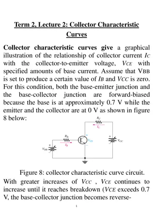
Working of UJT 1)Connect UJT with variable battery VE across emitter E & base B1and fixed battery VBB across base terminalsB1B2 as shown in fig4. 2) VE act as a variable i/p voltage source and VBB provides a constant voltage from B2 to B1. 3)As long as VE is less than VRB1,the p-n junction will remain reverse biased ,hence the UJT will stays in the OFF state. 4)In this state only reverse leakage current will flows from B2 to emitter E. 5)As VE approaches VP(peak point voltage),the p-n junction becomes forward biased and emitter current IE flows from emitter E to base B1.This means UJT starts conducting in the opposite direction.
The V-I characteristics of UJT are shown in fig5.From this fig following points may be observed. 1)The region to the left of peak point is called as cut- off region. In this region the emitter current IE is very small which is a leakage current flowing from B2 to emitter. 2)At VE=VP ,the UJT starts conducting and hence VE starts decreasing with the increase in IE .This property will be observed up to the valley point VV .This region of device is called as negative resistance region. 3)After the valley point the device enter in to the saturation region where IE increase with increase in VE. V-I Characteristics of UJT:- fig5
6)At this point holes from the heavily doped emitter region are injected into the n-type bar & they move towards B1 terminal .Hence the resistance RB1 is drastically reduced 7)The decrease in RB1 decreases VRB1(i.e.VE)and hence increases the forward biased 8)The increase forward biased increases emitter current IE and decreases emitter voltage VE even further up to the valley point. This is the negative resistance region of the device 8)After valley point ,any increase in IE places the device in saturation.
Important parameters of UJT :- 1)Peak point voltage(Vp):-It is the emitter voltage that is required to trigger or to start conducting the UJT device. It is given by the equation VP = *VBB+VD 2) Peak point current (Ip):-It is the minimum emitter current that is required to trigger or to starts conducting the UJT device. 3) Valley point voltage(Vv):-It is the emitter voltage at the valley point. Its value increase with the increase in inter base voltage VBB. 4) Valley point current(Iv):-It is the emitter current at the valley point. Its value increase with the increase in inter base voltage VBB. 5) Inter base resistance (RBB):-It is the total resistance of the UJT device across B1 & B2 terminals. It is given by the equation RBB = RB1 + RB2 6)Intrinsic stand-off ratio ( ):-It is the ratio of RB1 to the total device resister RBB. It is in the range of 0.51 to 0.82 It is given by the equation =(RB1/RB1+RB2) =(RB1/RBB)
UJT as a Relaxation oscillator:- 1) Fig.6 shows UJT relaxation oscillator where the discharging of a capacitor through UJT can develop a saw tooth waveforms at output . When battery VBB is turned on , the capacitor C charges through resistor R. During charging period the voltage across the capacitor increases in an exponential manner as shown in fig.6 until it reaches the peak point voltage. Now at peak point voltage UJT is fired and capacitor discharges through UJT as shown in fig.6 As the capacitor voltage become zero ,the UJT is switched off. Again next cycle begins allowing the capacitor C to charge again. Thus UJT develop a saw tooth waveforms at output . The frequency of saw tooth waveform is given by Time period t = 2.3RCLoge(1/1- ) sec Frequency f = 1/t Hz 2) 3) 4) 5) 6)
UJT Relaxation Oscillator Positive spikes
Application of UJT:- UJT can be used in the following applications 1)It is used to trigger SCRs and TRIACS 2) It is used in non sinusoidal oscillators 3) It is used in phase control and timing circuits 4) It is used in saw tooth generators 5) It is used in high switching speed applications


At this point holes from the heavily")