▣ PTC Current Measurement Simulation (200V/V)
This simulation involves measuring current using a PTC device in a basic schematic setup with various components such as resistors, transistors, capacitors, and voltage sources. The simulation includes scenarios with high voltage, gate voltage variations, and overcurrent conditions. Different configurations and voltage levels are tested to understand the behavior of the system under varying conditions.

Download Presentation

Please find below an Image/Link to download the presentation.
The content on the website is provided AS IS for your information and personal use only. It may not be sold, licensed, or shared on other websites without obtaining consent from the author.If you encounter any issues during the download, it is possible that the publisher has removed the file from their server.
You are allowed to download the files provided on this website for personal or commercial use, subject to the condition that they are used lawfully. All files are the property of their respective owners.
The content on the website is provided AS IS for your information and personal use only. It may not be sold, licensed, or shared on other websites without obtaining consent from the author.
E N D
Presentation Transcript
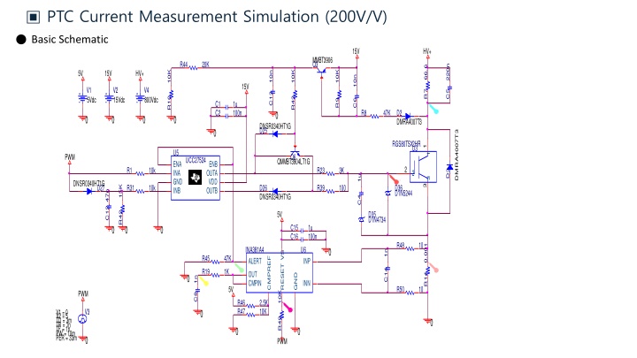
PTC Current Measurement Simulation (200V/V) Basic Schematic 15V HV+ MMBT3906 R44 20K Q3 220n 66.6 5V 15V HV+ 10K 10K 10K 10n 10n 15V V1 5Vdc V2 15Vdc V4 800Vdc R7 C5 C13 R10 R43 R9 C6 C1 C2 1u 100n R8 47K D2 DMRA4007T3 V 0 0 0 0 0 DNSR0340HT1G D25 0 DMRA4007T3 RGS80TSX2HR U3 11 U5 ENA PWM Q6 UCC27524 QMMBT3904LT1G ENB 2 R1 10k R23 3K INA GND OUTA VDD 2 D3 1u 3 DNSR0340HT1G V D27 R31 10k D26 DNSR0340HT1G R39 100 D36 D1N5244 3 15K INB OUTB C12 47n C4 5V D35 D1N4734 R42 C15 C16 1u 100n 0 0 0 R48 10 0.001 INA381A4 ALERT U6 INP 0 1n VS R45 47K CMPREF RESET R19 1K C14 V I OUT R14 GND 0 1n CMPIN INN V 5V R50 10 PWM 10K C8 R46 R47 2.5K 10K V3 V V1 = 0 V2 = 5 0 TD = 3m TF = 1n PW = 10m PER = 33m R49 0 TR = 1n 0 0 0 PWM
Simulation : High Voltage = 800V, Gate Voltage = 15V, PTC = 66.6(12.01A) IGBT Collector Voltage (50:1) IGBT Gate Voltage HV Current INA381A4 : RESET INA381A4 : ALERT INA381A4 : OUT
Overcurrent condition 15V HV+ MMBT3906 R44 20K Q3 220n 33.3 5V 15V HV+ 10K 10K 10K 10n 10n 15V V1 5Vdc V2 15Vdc V4 800Vdc R7 C5 C13 R10 R43 R9 C6 C1 C2 1u 100n R8 47K D2 DMRA4007T3 V 0 0 0 0 0 DNSR0340HT1G D25 0 DMRA4007T3 RGS80TSX2HR U3 11 U5 ENA PWM Q6 UCC27524 QMMBT3904LT1G ENB 2 R1 10k R23 3K INA GND OUTA VDD 2 D3 1u 3 DNSR0340HT1G V D27 R31 10k D26 DNSR0340HT1G R39 100 D36 D1N5244 3 15K INB OUTB C12 47n C4 5V D35 D1N4734 R42 C15 C16 1u 100n 0 0 0 R48 10 0.001 INA381A4 ALERT U6 INP 0 1n VS R45 47K CMPREF RESET R19 1K C14 V I OUT R14 GND 0 1n CMPIN INN V 5V R50 10 PWM 10K C8 R46 R47 2.5K 10K V3 V V1 = 0 V2 = 5 0 TD = 3m TF = 1n PW = 10m PER = 33m R49 0 TR = 1n 0 0 0 PWM
Simulation : High Voltage = 800V, Gate Voltage = 15V, PTC = 33.3(24.02A) IGBT Collector Voltage (50:1) INA381A4 : RESET (H = Latch Mode) INA381A4 : ALERT (Transparent??)
Overcurrent condition (INA381 Gate Driver disconnected) 15V HV+ MMBT3906 R44 20K Q3 220n 33.3 5V 15V HV+ 10K 10K 10K 10n 10n 15V V1 5Vdc V2 15Vdc V4 800Vdc R7 C5 C13 R10 R43 R9 C6 C1 C2 1u 100n R8 47K D2 DMRA4007T3 V 0 0 0 0 0 DNSR0340HT1G D25 0 DMRA4007T3 RGS80TSX2HR U3 11 U5 ENA PWM Q6 UCC27524 QMMBT3904LT1G ENB 2 R1 10k R23 3K INA GND OUTA VDD 2 D3 1u 3 DNSR0340HT1G V D27 R31 10k D26 DNSR0340HT1G R39 100 D36 D1N5244 3 15K INB OUTB C12 47n C4 5V D35 D1N4734 R42 C15 C16 1u 100n 0 0 0 5V R48 10 0.001 INA381A4 ALERT U6 INP 0 1n VS R45 47K CMPREF RESET R19 1K C14 V I OUT R14 GND 1n CMPIN INN V 5V R50 10 PWM 10K C8 R46 R47 2.5K 10K V3 V V1 = 0 V2 = 5 0 TD = 3m TF = 1n PW = 10m PER = 33m R49 0 TR = 1n 0 0 0 PWM
Simulation : High Voltage = 800V, Gate Voltage = 15V, PTC = 33.3(24.02A) HV Current IGBT Collector Voltage (50:1) IGBT Gate Voltage INA381A4 : RESET (H = Latch Mode) Transparent Mode (RESET = L) INA381A4 : OUT INA381A4 : ALERT
Overcurrent Condition (5V INA381 RESET) 15V HV+ MMBT3906 R44 20K Q3 220n 33.3 5V 15V HV+ 10K 10K 10K 10n 10n 15V V1 5Vdc V2 15Vdc V4 800Vdc R7 C5 C13 R10 R43 R9 C6 C1 C2 1u 100n R8 47K D2 DMRA4007T3 V 0 0 0 0 0 DNSR0340HT1G D25 0 DMRA4007T3 RGS80TSX2HR U3 11 U5 ENA PWM Q6 UCC27524 QMMBT3904LT1G ENB 2 R1 10k R23 3K INA GND OUTA VDD 2 D3 1u 3 DNSR0340HT1G V D27 R31 10k D26 DNSR0340HT1G R39 100 D36 D1N5244 3 15K INB OUTB C12 47n C4 5V D35 D1N4734 R42 C15 C16 1u 100n 0 0 0 5V R48 10 0.001 INA381A4 ALERT U6 INP 0 1n VS R45 47K CMPREF RESET R19 1K C14 V I OUT R14 GND 1n CMPIN INN V 5V R50 10 PWM 10K C8 R46 R47 2.5K 10K V3 V V1 = 0 V2 = 5 0 TD = 3m TF = 1n PW = 10m PER = 33m R49 0 TR = 1n 0 0 0 5V
Simulation : High Voltage = 800V, Gate Voltage = 15V, PTC = 33.3(24.02A) HV Current IGBT Collector Voltage (50:1) IGBT Gate Voltage INA381A4 : RESET (H = Latch Mode) INA381A4 : OUT INA381A4 : ALERT Latch Mode (Low )
Questions 1. INA381 does not enter latch mode 1) Operating conditions: The MCU output PWM signal is connected to the reset pin of INA381, and when PWM on, the reset pin is also high, so it is expected to operate in latch mode 2) Expected behavior: If an overcurrent occurs when the gate driver's IN is on (PWM On), the alert output of INA381 changes the EN of the gate driver to the low state, causing the gate driver to go off I want SelfFailsafe operation, not PWM off by monitoring alert status in MCU. 3) Simulation results INA381 and Gate Driver Interworking: Operation in Transparent Mode even though Reset Pin is High INA381 and Gate Driver not interlocked: Expected to operate in latch mode (Difficult to accurately verify by connecting PWM to RESET) Input 5V to INA381 RESET: Confirm that it is operating in latch mode (Alert = Low state is maintained even when PWM is off) Estimated IGBT loss when operating as shown in even if the actual circuit is configured Need to check if it works the same way when configuring the actual circuit 4) Request for TI review Review simulation conditions: Even when PWM and RESET are linked, it seems to be a latch mode condition when PWM = ON, so why does it operate like Transparent Mode? Whether there is a difference in simulation from the actual product: request for library review, INA381 EVM application completed (action will be checked after receipt) 2. 2. OPAMP Current Sense Amplifier change review 1) OPAMP Performance Comparison (ST TSZ121 VS TI OPA317): When the actual current is 0A, ST TSZ121 is advantageous based on output error ST TSZ121 (Offset Voltage: Max 8uV): 0A Maximum Output 0.22mV (40 samples) TI Company OPA317 (Offset Voltage: Max 100uV): 0A Maximum Output 1.09 mV (40 samples) TI TLV9062 (Offset Voltage: Max 2,000uV): Maximum Output 28.53mV (40 samples) Very Good Not difficult to use Difficult to use 2) Current Sense Amplifier : Built-in resistance for amplifier circuit gives PCB mounting area advantage over OPAMP INA381A4QDGSRQ1(200V/V, O/V = 150uV) : Current Sense Amplifier + Overcurrent Comparator INA180A4QDBVRQ1 (200V/V, O/V = 150uV): Current Sense Amplifier Only Best if overcurrent is operated in latch mode Small mounting area compared to OPAMP configuration 3) Request for TI review Whether input filter configuration (serial resistance + capacitor) is also required when using loads of resistance components such as PTC heaters
")


")