Programmable Logic Arrays (PLA)

PLA (Programmable Logic
Array):
The combinational circuit do not use
all
the
minterms every
time. Occasionally,
they
have don't
care
conditions. Don't care condition when implemented
with
a
PROM
becomes
an
address input that will never
occur.
The result is that not all the
bit patterns available
in
the
PROM
are used, which may
be considered a
waste
of
available equipment.
For cases
where
the
number
of
don't
care
conditions is excessive, it
is
more
economical
to use a
second type
of
LSI component
called
a
Programmable Logic
Array (PLA).
A
PLA
is
similar to
a
PROM in concept; however it does not provide
full
decoding
of
the
variables
and
does
not
generates
all
the
min.
terms
as
in
the
PROM.
The PLA replaces decoder
by
group of AND gates, each
of
which can
be
programmed
to
generate
a
product term
of the
input variables.
In
PLA, both AND
and OR gates have fuses
at
the inputs,
therefore in
PLA both AND
and
OR
gates
are
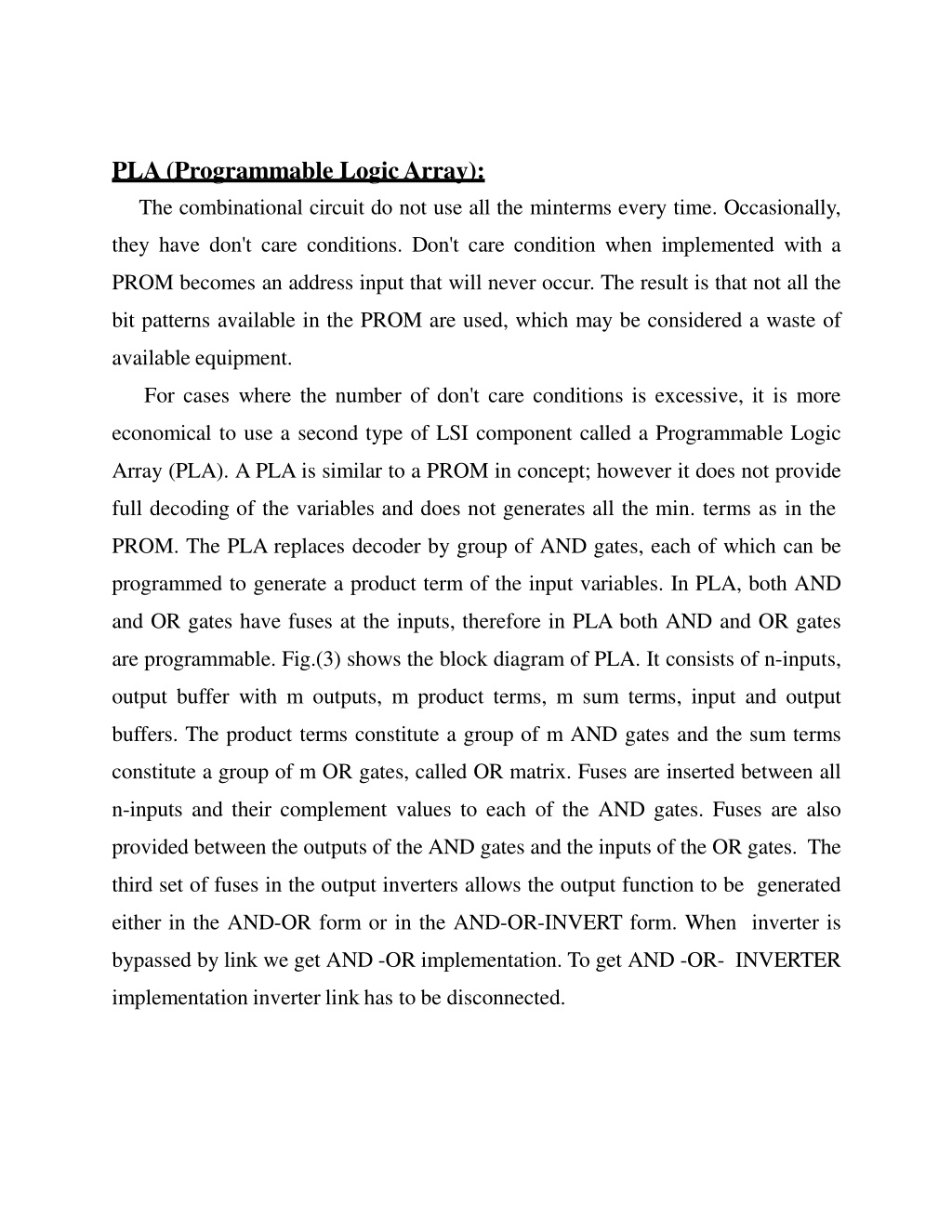
programmable. Fig.(3) shows the block diagram
of
PLA.
It
consists
of n-inputs,
output
buffer
with
m
outputs,
m
product terms,
m sum
terms, input and output
buffers. The product terms constitute
a
group
of
m
AND gates
and
the sum terms
constitute
a
group
of m
OR gates, called
OR
matrix. Fuses are inserted between all
n-inputs and their complement values
to each of the
AND gates. Fuses are
also
provided between the outputs
of
the
AND
gates and the inputs
of
the OR gates.
The third
set of
fuses in the output inverters allows the output function to be
generated either in the AND-OR
form or in
the AND-OR-INVERT form. When
inverter is bypassed
by
link we get AND -OR implementation. To get AND -OR-
INVERTER implementation inverter link
has
to
be
disconnected.

78
Fig.(3) Block
diagram of a
PLA
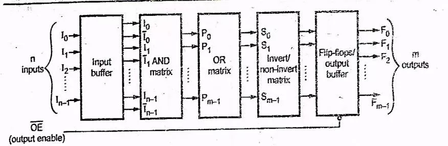
Input
Buffer:
Input
buffers
are
provided in
the
PLA
to
limit
loading
of
the sources that drive
the
inputs. They
also
provide inverted and non-inverted
form of
inputs
at
its
output.
Figure
(4) shows two ways
of
representing
input
buffer for single
input.
Fig. (4)
Input
buffer
for
single input
line
Output
Buffer:
The driving capacity
of
PLA is increased
by
providing buffers
at
the output.
They
are
usually
TTL
compatible.
Figure
(5)
shows
the
tri-state,
TTL
compatible
output buffer. The output
buffer
may provide
totem-pole,
open collector
or tri-state
output.
79
Fig.(5)
Output
buffers
Output
through
Flip-Flops:
For the
implementation of sequential circuits we need memory
elements,
flip-
flops
and
combinational circuitry
for
deriving the
flip-flop
inputs. To satisfy both
the
needs some PLAs
are
provided with
flip-flop at
each output,
as
shown in the
Fig.
(6).
Fig. (6) PLA
with
flip-flop
at the
output
80
Implementation
of
Combination
Logic
Circuit
using
PLA:
Like ROM, PLA
can be
mask-programmable
or
field-programmable. With
a
mask-programmable PLA,
the
user must
submit
a
PLA
program table to
the
manufacturer.
This
table
is
used
by the
vendor to produce
a user-made
PLA that
has
the required internal paths between inputs and outputs.
A
second type
of
PLA
available
is
called
a
field-programmable logic array
or
FPLA. The FPLA can be
programmed
by the
user
by
means
of
certain recommended procedures. FPLAs can
be
programmed with commercially available programmer
units.
As mentioned earlier, user has
to
submit PLA
program table
to the
manufacturers
to
get the
user-made
PLA.
Let us
study how
to
determine PLA
program table
with the help
of
example.
Example1
:
A
combinational circuit is defined
by the
functions
:
𝐹
1
=
∑
𝑚
(
3,5,7
)
𝐹
2
=
∑
𝑚
(
4,5,7
)
Implement the circuit with
a
PLA having
3
inputs,
3
product terms and two
outputs.
Solution
:
Let us determine the truth table
for
the given Boolean
functions
81
Table (1):
Truth
table
K-map
simplification
Fig. (7)
Table (2): PLA program
table
82
From
the
truth table, the Boolean functions are simplified,
as
shown in the
Figure.
The simplified functions
in
sum
of
products are obtained from
the
maps
are
:
𝐹
1
= 𝐴𝐶 +
𝐵𝐶
𝐹
2
=
𝐴𝐵
̅
+
𝐴𝐶
Therefore, there are three distinct product terms
:
AC,
BC
and
A
B̅
,
and
two
sum
terms. The PLA program table shown
in
Table
2
consists
of
three
columns
specifying product terms, inputs and outputs. The first
column
gives the lists
of
product
terms
numerically. The second column specifies the required
paths
between
inputs
and AND
gates.
The third column specifies
the
required
paths
between the AND gates and the OR gates. Under each output variable, we write
a T
(for
true)
if
the output inverter is to
be
bypassed, and
C (for
complement)
if
the
function
is
to
be
complemented
with
the output inverter. The product terms listed
on the
left
of
first
column
are not
the part
of
PLA
program table they are
included
for
reference
only.
Fig. (8)
83
Example 2
:
Illustrate how
a
PLA
can be
used for combinational logic design
with reference to the functions
:
𝑓
1
(
𝑎,
𝑏,
𝑐
)
=
∑
𝑚
(
0,1,3,4
)
𝑓
2
(
𝑎,
𝑏,
𝑐
)
=
∑
𝑚
(
1,2,3,4,5
)
Realize
the
same
assuming, that
a 3
×
4
×
2
PLA
is
available.
Solution
: K-map
simplification
Fig.
(9)
Table
(3)
84
Implementation
3 × 4 ×
2
Fig.
(10
)
Example3
:
Implement the following
multi
Boolean function using
PLA
PLD.
𝑓
1
(
𝑎
2
,
𝑎
1
,
𝑎
0
)
=
∑
𝑚
(
0,1,3,5
)
𝑎𝑛𝑑
𝑓
2
(
𝑎
2
,
𝑎
1
,
𝑎
0
)
=
∑
𝑚
(
3,5,7
)
Solution
:
Let us simplify
the
functions using
K-maps.
Fig.
(11)
85
𝒇
𝟏
=
𝒂̅
𝟐
𝒂̅
𝟏
+
𝒂̅
𝟐
𝒂
𝟎
+
𝒂̅
𝟏
𝒂
𝟎
𝒇
𝟐
=
𝒂
𝟐
𝒂
𝟎
+
𝒂
𝟏
𝒂
𝟎
To implement functions
f
1
and f
2
we require
3 × 5 × 2
PLA and we
have to
implement them using
3 × 4 × 2
PLA. Therefore, we have
to
examine
product
terms
by
grouping 0s instead
of 1.
That
is
product terms for complement
of a
function.
Fig.
(12)
𝑓
1̅
=
𝑎
2
𝑎̅
0
+
𝑎
1
𝑎̅
0
+
𝑎
2
𝑎
1
𝑓
2̅
=
𝑎̅
2
𝑎̅
1
+
𝑎
1
𝑎̅
0
+
𝑎
2
𝑎̅
0
Looking
at
function outputs we
can
realize that product terms
𝑎
2
𝑎̅
0
and
𝑎
1
𝑎̅
0
are
common
in
both functions. Therefore, we need only
4
product
terms
and functions
can
be
implemented using
a 3× 4 × 2
PLA
as
shown
in
Table (4)
and
Fig.
(13).
Table (4)
86
F
ig.
(13)
As shown in the
Fig.
(13)
exclusive-OR gate is programmed
to
invert the
function
to
get the desired function
outputs.
Example 4
:
Design
a
BCD to Excess-3 code converter
and
implement using
suitable PLA.
Solution
:
Let us derive the truth table
of BCD to Excess-3
converter
as
shown
in
Table
(5).
87
Table
(5)
Truth
table
for BCD
to Excess-
3 code
converter
88
Table
(6)
Fig.(14): BCD
to
Excess-3 code converter using PLA
Implementation
89
Fig.
(15)
Example 5
: A
combinational circuit
is defined
by
the
function
𝑭
𝟏
(
𝑨,
𝑩,
𝑪
)
=
∑
𝒎
(
𝟏, 𝟑,
𝟓
)
,
𝑭
𝟐
=
∑
𝒎
(
𝟐, 𝟒, 𝟓
)
Implement the circuit with
PLA
Solution
:
Let
us
determine truth table
for the
given Boolean
function.
90
Table (7):
Truth
table
Table (8): PLA program
table
K-map
simplification
91
Fig.
(16)
Example
6
:
92
Solution:
x
0
x
x
1
x
'
Fig.
(17)
93
Programmable Logic Arrays (PLAs) provide a flexible way to implement combinational circuits with don't care conditions efficiently. PLAs use programmable AND and OR gates to generate product terms, offering a more economical solution compared to PROMs for circuits with excessive don't care conditions. Learn about the structure and working of PLAs, including input and output buffers, output through flip-flops, and implementation examples using mask-programmable and field-programmable PLAs.

Download Presentation

Please find below an Image/Link to download the presentation.
The content on the website is provided AS IS for your information and personal use only. It may not be sold, licensed, or shared on other websites without obtaining consent from the author.If you encounter any issues during the download, it is possible that the publisher has removed the file from their server.
You are allowed to download the files provided on this website for personal or commercial use, subject to the condition that they are used lawfully. All files are the property of their respective owners.
The content on the website is provided AS IS for your information and personal use only. It may not be sold, licensed, or shared on other websites without obtaining consent from the author.
E N D
Presentation Transcript
PLA (Programmable LogicArray): The combinational circuit do not use all the minterms every time. Occasionally, they have don't care conditions. Don't care condition when implemented with a PROM becomes an address input that will never occur. The result is that not all the bit patterns available in the PROM are used, which may be considered a waste of available equipment. For cases where the number of don't care conditions is excessive, it is more economical to use a second type of LSI component called a Programmable Logic Array (PLA). A PLA is similar to a PROM in concept; however it does not provide full decoding of the variables and does not generates all the min. terms as in the PROM. The PLA replaces decoder by group of AND gates, each of which can be programmed to generate a product term of the input variables. In PLA, both AND and OR gates have fuses at the inputs, therefore in PLA both AND and OR gates are programmable. Fig.(3) shows the block diagram of PLA. It consists of n-inputs, output buffer with m outputs, m product terms, m sum terms, input and output buffers. The product terms constitute a group of m AND gates and the sum terms constitute a group of m OR gates, called OR matrix. Fuses are inserted between all n-inputs and their complement values to each of the AND gates. Fuses are also provided between the outputs of the AND gates and the inputs of the OR gates. The third set of fuses in the output inverters allows the output function to be generated either in the AND-OR form or in the AND-OR-INVERT form. When inverter is bypassed by link we get AND -OR implementation. To get AND -OR- INVERTER implementation inverter link has to be disconnected.
78 Fig.(3) Block diagram of a PLA InputBuffer: Input buffers are provided in the PLA to limit loading of the sources that drive the inputs. They also provide inverted and non-inverted form of inputs at its output. Figure (4) shows two ways of representing input buffer for single input. Fig. (4) Input buffer for single input line OutputBuffer: The driving capacity of PLA is increased by providing buffers at the output. They are usually TTL compatible. Figure (5) shows the tri-state, TTL compatible
output buffer. The output buffer may provide totem-pole, open collector or tri-state output. 79 Fig.(5) Outputbuffers Output throughFlip-Flops: For the implementation of sequential circuits we need memory elements, flip- flops and combinational circuitry for deriving the flip-flop inputs. To satisfy both the needs some PLAs are provided with flip-flop at each output, as shown in the Fig. (6).
Fig. (6) PLA with flip-flop at the output 80 ImplementationofCombinationLogicCircuitusingPLA: Like ROM, PLA can be mask-programmable or field-programmable. With a mask-programmable PLA, the user must submit a PLA program table to the manufacturer. This table is used by the vendor to produce a user-made PLA that has the required internal paths between inputs and outputs. A second type of PLA available is called a field-programmable logic array or FPLA. The FPLA can be programmed by the user by means of certain recommended procedures. FPLAs can be programmed with commercially available programmer units. As mentioned earlier, user has to submit PLA program table to the manufacturers to get the user-made PLA. Let us study how to determine PLA program table with the help of example. Example1: A combinational circuit is defined by the functions : ?1 = ?(3,5,7)
?2 = ?(4,5,7) Implement the circuit with a PLA having 3 inputs, 3 product terms and two outputs. Solution : Let us determine the truth table for the given Boolean functions 81 Table (1): Truth table A B C F1 F2 0 0 0 0 0 0 0 1 0 0 0 1 0 0 0 0 1 1 1 0 1 0 0 0 1 1 0 1 1 1 1 1 0 0 0 1 1 1 1 1 K-mapsimplification
Fig. (7) Table (2): PLA program table Product Inputs Outputs term A B C F1 F2 1 1 - 1 1 1 2 - 1 1 1 - 3 1 0 - - 1 T T T/C 82 From the truth table, the Boolean functions are simplified, as shown in the Figure. The simplified functions in sum of products are obtained from the maps are : ?1 = ?? + ?? ?2 = ?? + ?? Therefore, there are three distinct product terms : AC, BC and AB , and two sum terms. The PLA program table shown in Table 2 consists of three columns specifying product terms, inputs and outputs. The first column gives the lists of product terms numerically. The second column specifies the required paths between inputs and AND gates. The third column specifies the requiredpaths
between the AND gates and the OR gates. Under each output variable, we write a T (for true) if the output inverter is to be bypassed, and C (for complement) if the function is to be complemented with the output inverter. The product terms listed on the left of first column are not the part of PLA program table they are included for reference only. Fig. (8) 83 Example 2 : Illustrate how a PLA can be used for combinational logic design with reference to the functions : ?1(?, ?, ?) = ?(0,1,3,4) ?2(?, ?, ?) = ?(1,2,3,4,5)
Realize the same assuming, that a 342 PLA is available. Solution: K-map simplification Fig. (9) Table(3) Inputs Outputs Product terms A b 0 c 0 F1 1 F2 - ? ? - 0 1 0 1 0 1 - - 1 - - T 1 1 1 T ? c c a a? ? b b 84 Implementation
Fig. (10) Example3: Implement the following multi Boolean function using 3 4 2 PLAPLD. ?1(?2, ?1, ?0) = ?(0,1,3,5)??? ?2(?2, ?1, ?0) = ?(3,5,7) Solution : Let us simplify the functions usingK-maps.
Fig. (11) 85 ??= ? ?? ?+ ? ???+ ? ??? ??= ????+???? To implement functions f1 and f2 we require 3 5 2 PLA and we have to implement them using 3 4 2 PLA. Therefore, we have to examine product terms by grouping 0s instead of 1. That is product terms for complement of a function. Fig. (12) ?1 = ?2? 0 + ?1? 0 + ?2?1 ?2 = ? 2? 1 + ?1? 0 +?2? 0 Looking at function outputs we can realize that product terms ?2? 0and ?1? 0are common in both functions. Therefore, we need only 4 product terms and functions can be implemented using a 3 4 2 PLA as shown in Table (4) and Fig. (13). Table (4) Inputs Outputs Product terms ?2 1 - 1 0 ?1 - 1 1 0 ?0 0 0 - - ?1 1 1 1 - C ?2 1 1 ?2? 0 ?1? 0 ?2?1 ? 2? 1 1 C
86 Fig. (13) As shown in the Fig. (13) exclusive-OR gate is programmed to invert the function to get the desired function outputs.
Example 4 : Design a BCD to Excess-3 code converter and implement using suitable PLA. Solution : Let us derive the truth table of BCD to Excess-3 converter as shown in Table (5). 87 Table (5) Truth table for BCD to Excess- 3 code converter
88 Table(6)
Fig.(14): BCD to Excess-3 code converter using PLA Implementation
89 Fig.(15) Example 5 : A combinational circuit is defined by the function ??(?, ?, ?) = ?(?, ?,?), ??= ? (?, ?, ?) Implement the circuit with PLA
Solution: Let us determine truth table for the given Boolean function. 90 Table (7): Truth table B C A F1 F2 0 0 0 0 0 0 0 1 1 0 0 1 0 0 1 0 1 1 1 0 1 0 0 0 1 1 0 1 1 1 1 1 0 0 0 1 1 1 0 0 Table (8): PLA program table K-mapsimplification
91 Fig.(16)
Example 6: Solution: x 0= x x 1= x' 92
Fig.(17) 93
:")


 PLA with flip-flop at the output")
")
")


")
")


: BCD to Excess-3 code converter using PLA")


")