Printed Circuit Board (PCB) Fabrication
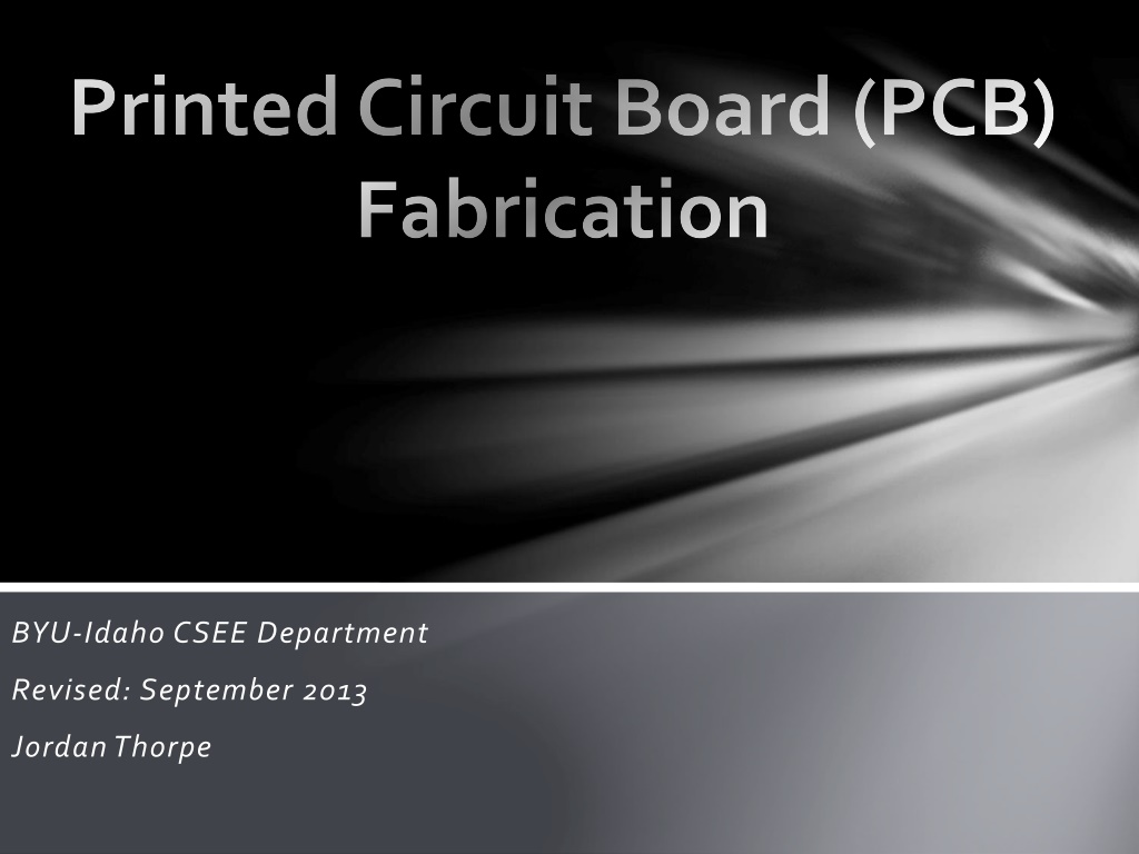
BYU-Idaho CSEE Department
Revised: September 2013
Jordan Thorpe
Find/Create Schematic
Drawing
Draw it in Multisim
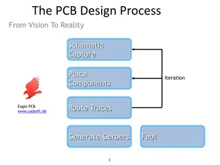
Fabrication Process Overview (6 Steps)
Step 1
Step 2
http://worldtechnical.blogspot.com/2009/07/
led-chaser-circuit.html#.Uhjw1j-Pi8B
Transfer to Ultiboard
Arrange parts on board layout
Fabrication Process Overview (6 Steps)
Step 3
Step 4
Add traces between pads
Bring .ewprj file to lab
assistant
at LPKF station
in
AUS 202
Fabrication Process Overview (6 Steps)
Step 5
Step 6
Multisim
Multisim: Placing Components
You must select a footprint!
…or else the
part will be
black when
placed and will
not transfer to
Ultiboard!
Multisim’s
Component Wizard
has 6 steps to creating your own components.
Step 1: Give your part a name and select what information you will provide
Multisim: Creating Components
Step 2: Enter footprint information (ie. Number of pins and sections)
Step 3: Design a symbol for your part
Multisim: Creating Components (cont.)
Step 4: Set pin parameters
Step 5: Assign part pins to footprint pins (Click on
Map Pins
, then
Auto-assign
)
Multisim: Creating Components (cont.)
Step 6: Save your new part to the
User Database
and click
Finish
You can now place your part in Multisim!
Multisim: Creating Components (cont.)
Multisim: Assigning Footprints
GREEN
Pads are
Surface Mount
Components
BLUE
Pads are
Through-Hole
Components
Double click on any wire to see its Net Name
Net Names in Multisim are the same as the
names in Ultiboard
Do you want to create a place to input external
wires into your PCB? Use the “Test Point” part:
Multisim: Wires & Nets
You can simulate your circuit as long as all
of the components you are using have
simulation models. If they don’t you will
have to write your own scripts for them.
During simulations, you can flip switches,
adjust potentiometers, etc. to see if your
circuit acts as expected.
When I simulated the circuit, I could see
the LEDs flickering, but in the screen shot
I took, only one is illuminated, as
expected.
Multisim: Simulation
When transferring to Ultiboard,
you will be prompted to save
the .ewnet file. Save it with
your .ms12 multisim file
because whenever you
forward/backward annotate,
you will select the .ewnet file to
update it.
Multisim: Transferring to Ultiboard
** This is the first screen you will
see in Ultiboard after transferring
Ultiboard
When using Ultiboard, remember to save often! There are a few unknown
things that throw an Unhandled win32 Exception and crash the program, so
if you haven’t saved your work, it will be lost.
A Word of Caution:
Select
Parts
Select
Traces
Select
Copper Areas
such as Teardrops
Select
Vias
Select
THT Pads
(Through hole)
Select
SMT Pads
(Surface Mount)
Select
Text/Attributes
Select
Miscellaneous
such as board outline and dimensions
Ultiboard: Selection Palette
1) Make sure that the miscellaneous selector is down.
2) Right click on the yellow outline and select properties.
Either:
3) Click on the “Rectangle” tab and enter dimensions
-0r-
3) Click “Cancel” and then adjust
the size of the yellow box manually
Ultiboard: Set Board Size
After you transfer to Ultiboard, all of your components will be placed together with
yellow lines connecting them. This is called the “ratsnest”.
Wires in Multisim are represented by yellow lines in Ultiboard.
When you move parts in Ultiboard, the yellow lines will move with the part to show
you how it connects with other parts.
Move the parts and arrange them how you would like on your PCB. Rule of thumb: it
is good to keep the yellow lines as short as possible! This will help make your traces
shorter, your board smaller and more professional.
Ultiboard: Piece Placement
In “In-Place Part Edit”, you can:
-
Move, add, delete, or adjust a part’s
TEAL
silkscreen
-
Adjust the part’s footprint dimensions
-
Move a part’s pad and/or adjust its size/diameter
-
Use the dimension tool to ensure that the part will fit in the footprint
-
Part dimensions can be found on the part’s Data Sheet.
You
cannot
change the name of the part in “In-Place Part Edit”
Ultiboard: In-Place Part Edit
All Drill Diameters less than 83 mils
must
be from the sizes shown on the chart below!
A couple helpful hints:
Use 24 mils for small capacitors and resistors
Use 31 mils for most resistors, integrated circuits, & vias
Use the calipers to find the diameter of your part
Make the drill diameter 5-10 mils larger than the part diameter
A good rule of thumb is to make the pad diameter close to triple
the diameter of the drill, and
no pad should be smaller than 70 mils
or else it will be nearly impossible to solder your part to the board.
Ultiboard: Pad/Via Drill Sizes
Placing Traces:
Automatic: Use the Auto-route button
Manual: Use Ctrl+T to manually place traces
GREEN
traces are milled onto the TOP of the board
RED
traces are milled onto the BOTTOM of the board
IMPORTANT:
Single-sided boards must only have
RED
traces!
Do you see
YELLOW
traces? That just means that there is a green trace
on the top in the same place that there is a red trace on the bottom.
Ultiboard: Traces
How do you make a trace go from the top layer to the bottom layer?
-Vias!
A via is a wire that goes through the PCB and is soldered on both sides.
Place a via with a red and green trace going to it.
Vias should have a drill diameter of 31 mils
and a pad diameter of 80 mils.
Ultiboard: Traces (cont.)
You should add “Teardrops” to each pad on your PCB.
Trace Width Calculator
ALL traces must be at least 31 mils wide!
Ultiboard: Traces (cont.)
http://circuitcalculator.com/wordpress/?p=25/
Make sure you have “Silkscreen Top” selected from the Design Toolbox on the left.
Next, select the text box and add your text. To make sure that the text
mills out correctly, make sure that it is “Thin” and at least 60 mils in size.
Text should appear
TEAL
in color. If it doesn’t check which layer you are in.
Note: You can also add text in “In-Place Part Edit” if the text is specific for a part.
Ultiboard: Placing Text
Forward Annotating
: If you are working in Ultiboard, and realize that there
is a mistake, you can go back to Multisim and fix it. Then, instead of
transferring
to Ultiboard, you can
forward annotate
to the Ultiboard file you
are already working on.
Back Annotating
: You can make minor changes in Ultiboard, such as name
changes, and then
back annotate
to Multisim and your changes will be saved
in your Multisim file.
Multisim/Ultiboard Annotation
Multisim
Ultiboard
DRC Check: Checks for design errors such as traces and parts that are too close
together.
Connectivity Check: Checks all nets and makes sure that they are connected
correctly.
Ultiboard: Error Checking
Your final product should look something like this:
Done!
Have you:
Verified that your circuit works on a Protoboard first?
Checked that the Vcc and Ground traces go to the correct pins on ICs, switches, etc?
Checked that all footprint dimensions are accurate? (i.e. your components will fit
snugly in the holes drilled for them?)
Checked all drill diameters so they are the right size?
Made sure that all traces are the correct thickness for your application?
Added teardrops to all traces when they enter a pad?
Made sure that if you are making a single sided board that all traces are
RED
?
Made sure that if you are making a double sided board that no
GREEN
trace crosses
a
TEAL
silkscreen?
If you can answer “Yes” to all these questions, bring your *.ewprj file on a USB drive to
the LPKF Lab Assistant in Lab 202.
Double-check the Following:
Have you:
Ran a Connectivity Check to make sure that all your pads are wired together
correctly? (And get no errors?)
Ran a DRC Errors Check to make sure that parts, pads, vias, and traces are not too
close together? (And get no errors?)
If you can answer “Yes” to all these questions, bring your *.ewprj file on a USB drive to
the LPKF Lab Assistant in Lab 202.
Double-check the Following: (cont.)
Circuit Cam
Board Master
Does anyone speak German?
LPKF stands for “Leiterplatten-Kopierfräsen”
which translates to “circuit board copy milling”.
LPKF
-
Mouser
-
Digi-key
-
Jameco
-
Newark
-
Farnell Element 14
-
Allied Electronics
Sourcing Components
Finished Product!
Multisim
http://www.ni.com/pdf/manuals/374483a.pdf
http://sine.ni.com/psp/app/doc/p/id/psp-412/lang/en
http://www.youtube.com/watch?v=pg4DI5s8FNo
Ultiboard
http://www.ni.com/pdf/manuals/374488a.pdf
http://sine.ni.com/psp/app/doc/p/id/psp-519/lang/en
http://www.youtube.com/watch?v=22j3u4BRTbs
More
http://www.youtube.com/watch?v=c1oCBJADJFQ
http://forums.ni.com/t5/Circuit-Design-Suite-Multisim/help-with-multisim-12/td-
p/2458896
For more information:
This content provides a detailed overview of the PCB fabrication process in 6 steps, including schematic drawing, part arrangement, trace addition, and more. It also guides on creating components in Multisim using the Component Wizard, emphasizing key steps like naming, footprint design, symbol creation, pin parameters, and saving to the User Database.

Download Presentation

Please find below an Image/Link to download the presentation.
The content on the website is provided AS IS for your information and personal use only. It may not be sold, licensed, or shared on other websites without obtaining consent from the author.If you encounter any issues during the download, it is possible that the publisher has removed the file from their server.
You are allowed to download the files provided on this website for personal or commercial use, subject to the condition that they are used lawfully. All files are the property of their respective owners.
The content on the website is provided AS IS for your information and personal use only. It may not be sold, licensed, or shared on other websites without obtaining consent from the author.
E N D
Presentation Transcript
Printed Circuit Board (PCB) Fabrication BYU-Idaho CSEE Department Revised: September 2013 Jordan Thorpe
Fabrication Process Overview (6 Steps) Step 1 Step 2 Find/Create Schematic Drawing Draw it in Multisim http://worldtechnical.blogspot.com/2009/07/ led-chaser-circuit.html#.Uhjw1j-Pi8B
Fabrication Process Overview (6 Steps) Step 3 Step 4 Transfer to Ultiboard Arrange parts on board layout
Fabrication Process Overview (6 Steps) Step 5 Step 6 Add traces between pads Bring .ewprj file to lab assistant at LPKF station in AUS 202
Multisim: Placing Components You must select a footprint! or else the part will be black when placed and will not transfer to Ultiboard!
Multisim: Creating Components Multisim sComponent Wizard has 6 steps to creating your own components. Step 1: Give your part a name and select what information you will provide
Multisim: Creating Components (cont.) Step 2: Enter footprint information (ie. Number of pins and sections) Step 3: Design a symbol for your part
Multisim: Creating Components (cont.) Step 4: Set pin parameters Step 5: Assign part pins to footprint pins (Click on Map Pins, then Auto-assign)
Multisim: Creating Components (cont.) Step 6: Save your new part to the User Database and click Finish You can now place your part in Multisim!
Multisim: Assigning Footprints GREEN Pads are Surface Mount Components BLUE Pads are Through-Hole Components
Multisim: Wires & Nets Double click on any wire to see its Net Name Net Names in Multisim are the same as the names in Ultiboard Do you want to create a place to input external wires into your PCB? Use the Test Point part:
Multisim: Simulation You can simulate your circuit as long as all of the components you are using have simulation models. If they don t you will have to write your own scripts for them. During simulations, you can flip switches, adjust potentiometers, etc. to see if your circuit acts as expected. When I simulated the circuit, I could see the LEDs flickering, but in the screen shot I took, only one is illuminated, as expected.
Multisim: Transferring to Ultiboard When transferring to Ultiboard, you will be prompted to save the .ewnet file. Save it with your .ms12 multisim file because whenever you forward/backward annotate, you will select the .ewnet file to update it. ** This is the first screen you will see in Ultiboard after transferring
A Word of Caution: When using Ultiboard, remember to save often! There are a few unknown things that throw an Unhandled win32 Exception and crash the program, so if you haven t saved your work, it will be lost.
Ultiboard: Selection Palette Select Parts Select Traces Select Copper Areas such as Teardrops Select Vias Select THT Pads (Through hole) Select SMT Pads (Surface Mount) Select Text/Attributes Select Miscellaneous such as board outline and dimensions
Ultiboard: Set Board Size 1) Make sure that the miscellaneous selector is down. 2) Right click on the yellow outline and select properties. Either: 3) Click on the Rectangle tab and enter dimensions -0r- 3) Click Cancel and then adjust the size of the yellow box manually
Ultiboard: Piece Placement After you transfer to Ultiboard, all of your components will be placed together with yellow lines connecting them. This is called the ratsnest . Wires in Multisim are represented by yellow lines in Ultiboard. When you move parts in Ultiboard, the yellow lines will move with the part to show you how it connects with other parts. Move the parts and arrange them how you would like on your PCB. Rule of thumb: it is good to keep the yellow lines as short as possible! This will help make your traces shorter, your board smaller and more professional.
Ultiboard: In-Place Part Edit In In-Place Part Edit , you can: - Move, add, delete, or adjust a part s TEAL silkscreen - Adjust the part s footprint dimensions - Move a part s pad and/or adjust its size/diameter - Use the dimension tool to ensure that the part will fit in the footprint - Part dimensions can be found on the part s Data Sheet. You cannotchange the name of the part in In-Place Part Edit
Ultiboard: Pad/Via Drill Sizes All Drill Diameters less than 83 mils must be from the sizes shown on the chart below! A couple helpful hints: Use 24 mils for small capacitors and resistors Use 31 mils for most resistors, integrated circuits, & vias Use the calipers to find the diameter of your part Make the drill diameter 5-10 mils larger than the part diameter A good rule of thumb is to make the pad diameter close to triple the diameter of the drill, and no pad should be smaller than 70 mils or else it will be nearly impossible to solder your part to the board.
Ultiboard: Traces Placing Traces: Automatic: Use the Auto-route button Manual: Use Ctrl+T to manually place traces GREEN traces are milled onto the TOP of the board RED traces are milled onto the BOTTOM of the board IMPORTANT: Single-sided boards must only have RED traces! Do you see YELLOW traces? That just means that there is a green trace on the top in the same place that there is a red trace on the bottom.
Ultiboard: Traces (cont.) How do you make a trace go from the top layer to the bottom layer? -Vias! A via is a wire that goes through the PCB and is soldered on both sides. Place a via with a red and green trace going to it. Vias should have a drill diameter of 31 mils and a pad diameter of 80 mils.
Ultiboard: Traces (cont.) You should add Teardrops to each pad on your PCB. Trace Width Calculator ALL traces must be at least 31 mils wide! http://circuitcalculator.com/wordpress/?p=25/
Ultiboard: Placing Text Make sure you have Silkscreen Top selected from the Design Toolbox on the left. Next, select the text box and add your text. To make sure that the text mills out correctly, make sure that it is Thin and at least 60 mils in size. Text should appear TEALin color. If it doesn t check which layer you are in. Note: You can also add text in In-Place Part Edit if the text is specific for a part.
Multisim/Ultiboard Annotation Forward Annotating: If you are working in Ultiboard, and realize that there is a mistake, you can go back to Multisim and fix it. Then, instead of transferring to Ultiboard, you can forward annotate to the Ultiboard file you are already working on. Back Annotating: You can make minor changes in Ultiboard, such as name changes, and then back annotate to Multisim and your changes will be saved in your Multisim file. Multisim Ultiboard
Ultiboard: Error Checking DRC Check: Checks for design errors such as traces and parts that are too close together. Connectivity Check: Checks all nets and makes sure that they are connected correctly.
Done! Your final product should look something like this:
Double-check the Following: Have you: Verified that your circuit works on a Protoboard first? Checked that the Vcc and Ground traces go to the correct pins on ICs, switches, etc? Checked that all footprint dimensions are accurate? (i.e. your components will fit snugly in the holes drilled for them?) Checked all drill diameters so they are the right size? Made sure that all traces are the correct thickness for your application? Added teardrops to all traces when they enter a pad? Made sure that if you are making a single sided board that all traces are RED? Made sure that if you are making a double sided board that no GREEN trace crosses a TEAL silkscreen? If you can answer Yes to all these questions, bring your *.ewprj file on a USB drive to the LPKF Lab Assistant in Lab 202.
Double-check the Following: (cont.) Have you: Ran a Connectivity Check to make sure that all your pads are wired together correctly? (And get no errors?) Ran a DRC Errors Check to make sure that parts, pads, vias, and traces are not too close together? (And get no errors?) If you can answer Yes to all these questions, bring your *.ewprj file on a USB drive to the LPKF Lab Assistant in Lab 202.
LPKF Does anyone speak German? LPKF stands for Leiterplatten-Kopierfr sen which translates to circuit board copy milling .
Sourcing Components - Mouser - Digi-key - Jameco - Newark - Farnell Element 14 - Allied Electronics
For more information: Multisim http://www.ni.com/pdf/manuals/374483a.pdf http://sine.ni.com/psp/app/doc/p/id/psp-412/lang/en http://www.youtube.com/watch?v=pg4DI5s8FNo Ultiboard http://www.ni.com/pdf/manuals/374488a.pdf http://sine.ni.com/psp/app/doc/p/id/psp-519/lang/en http://www.youtube.com/watch?v=22j3u4BRTbs More http://www.youtube.com/watch?v=c1oCBJADJFQ http://forums.ni.com/t5/Circuit-Design-Suite-Multisim/help-with-multisim-12/td- p/2458896
")
")
")
")
")


")
")
")


")
")


")