Diodes: Basics and Applications
Electronic
Prof. Dr. Ehssan Al-Bermany
Asst.lect Israa Hussein
1
s
t
s
e
m
e
s
t
e
r
Chapter three
Diode and its Application
Lecture 3
2
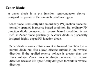
Diode
Diode
is a
semiconductor
device,
made
from a
small piece of
semiconductor material
, such as
silicon
.
It is consist of
two part
that divided in equal, the
first
half
is doped as a
p region
and
second half
is doped as an
n region
.
Theses two part with the depletion region in between produced the
pn
junction.
The
p region
is called the
anode
and
n region
is called the
cathode
.
It conducts
current
in
one direction
and offers
high resistance
in
other
direction
. The basic diode structure and symbol are shown in Fig.1.
3
Forward Bias
Bias
is the application of a
dc voltage to a diode
to make it either
conduct current or not
.
Forward bias
is the condition that allows current through the pn
junction. This external bias voltage is designated as VBIAS.
The
resistor limits
the
forward current
to a value that
will not damage
the diode
.
In the
forward bias
, the
negative side
of VBIAS is connected to the
n
region
of the diode and the
positive side is connected to the p region
. The
bias voltage
VBIAS,
must be greater
than the
barrier potential
; bias
must be greater than
0.3V for germanium
or
0.7V for silicon
diodes.
4
Negative side
of bias voltage ‘
pushes
’
free electrons towards pn junction
.
The
negative side of the source
also
provides
a
continuous flow of electrons
through
the external connection (conductor) and into the n region as shown in Figure 3.
The
bias-voltage source
imparts
sufficient energy to the
free electrons
for them to
overcome the barrier potential of the depletion region and move on through into the p
region.
Since unlike charges attract, the
positive side of the bias-voltage source
attracts
the
valence electrons
toward the
left end of the p region
.
The holes in the p region provide the medium for these valence electrons to move
through the p region. The holes, (majority in p region), move to the right toward the
junction.
As the electrons flow out of the p region through the external connection (conductor),
these electrons
become
conduction electrons
in the
metal conductor
.
As
more electrons move into the depletion region
, the number of
positive ions is
reduced
.
As more holes flow into the depletion region
on the other side of the pn junction, the
number of negative ions is reduced
.
This
reduction in positive and negative ions causes
the depletion region to narrow.
5
Reverse Bias
Reverse bias
is the condition that essentially
prevents current
through
the diode. Figure 4 shows a dc voltage source connected across a diode
in the direction to produce reverse bias.
The
positive side
of VBIAS is
connected
to the
n region
of the diode and
the
negative side
is connected to the
p region
.
Also,
note
that the
depletion region
is shown
much wider
than in
forward bias or equilibrium.
The
positive side
of the
bias-voltage source
pulls
the
free electrons
,
(
majority in n region
),
away
from the
pn junction
.
As electrons move away from junction,
more positive ions
are
created
.
This
results
in a
widening of the depletion region
and a
depletion of
majority carriers
.
6
Reverse Bias
In p region,
electrons from negative side
of
battery
enter as
valence
electrons
. It
moves
from
hole
to
hole
toward the
depletion region
,
creating
more negative ions
.
This can be viewed as
holes being pulled
towards
the
negative side
.
The
electric
field
increases
in
strength
until the potential
across
the
depletion region equals the bias voltage
.
At this point, very small
reverse current
exist
that can usually be
neglected
.
7
Voltage-Current (V-I) Characteristic of A Diode
V-I Characteristic for Forward Bias
The
current in forward biased
called
forward current
and is
designated
If.
At 0V
(Vbias) across the diode, there is
no forward current
. Figure 5
illustrates what happens as the forward-bias voltage is increased
positively from 0 V.
The
resistor is used
to
limit the forward current to a value
that will
not
overheat the diode and cause damage
.
Figure 5
: Relationship of voltage and current in a
forward-biased diode.
8
With
gradual increase of Vbias
, the
forward voltage
and
forward current
increases
.
A portion of
forward-bias voltage (Vf) drops
across the
limiting resistor.
Continuing
increase of Vf
causes
rapid increase of
forward current
but
the
voltage
across the diode
increases
only
gradually
above 0.7V.
The
resistance of the forward-biased
diode is
not constant
but
it changes over the entire curve.
Therefore, it is
called dynamic resistance.
9
V-I Characteristic for Reverse Bias
With
0V reverse voltage
there is
no reverse current
.
There is
only
a
small current through the junction
as the
reverse voltage increases
.
At a point
,
reverse current
shoots up
with the breakdown
of diode. The voltage called
breakdown voltage
.
This is
not normal mode of operation
.
After this point
the
reverse voltage remains at
approximately VBR
but
IR increase very rapidly
.
Break down voltage
depends
on
doping level
, set by
manufacturer.
10
Combine the curves for both forward bias and reverse bias, and you
have the
complete V-I characteristic
curve for a diode, as shown in
Figure 6.
11
Diode models
The
Ideal
Diode Mode
1- When the diode is
forward-biased
, it ideally acts like a
closed (on) switch
,
as shown in Figure 7.
2- When the diode is
reverse-biased
, it ideally acts like an
open (off) switch
,
as shown in part (
b
).
The barrier potential, the forward dynamic resistance, and the reverse current
are all neglected.
In Figure 7c, the ideal V-I characteristic curve graphically depicts the ideal
diode operation.
12
The Practical Diode Model
The
practical model
includes the
barrier potential
. The
characteristic curve for the practical diode model is shown in Figure
8c.
Since the
barrier potential
is included and
the dynamic resistance
is neglected
, the diode is assumed to have a voltage across it when
forward-biased, as indicated by the curve to the right of the origin.
The
practical model
is useful in
lower-voltage circuits
and in
designing basic diode
circuits. The
forward current
is determined
using
first Kirchhoff’s voltage law
to Figure 8a:
13
14
Example 1: (a) Determine the forward voltage and forward current for the
diode in Figure 10 (a) for each of ideal and practical diode models. Also, find
the voltage across the limiting resistor in each case.
(b) Determine the reverse voltage and reverse current for the diode in Figure
10(b) for each of the diode models. Also, find the voltage across the limiting
resistor in each case. Assume IR = 1μA. (H.W.)
15
The DC power supply
A
power supply
is an essential part of each electronic system from the
simplest to the most complex. A basic block diagram of the complete
power supply is shown in the below Figure.
The
transformer changes
ac voltages based
on the
turns ratio
between
the
primary
and
secondary
.
The
rectifier converts
the
ac input voltage
to
dc voltage
.
The
filter eliminates
the fluctuations in the rectified voltage and
produces a
relatively smooth dc voltage.
The
regulator
is a
circuit
that maintains a
constant
dc voltage
for
variations in the input line voltage or in the load
.
16
Half-Wave Rectifiers
Because of their
ability
to
conduct current in one direction
and
block current in
the other direction
, diodes are used in circuits called rectifiers that convert
AC
voltage into
DC
voltage.
Rectifiers
are found in all
dc power
supplies that operate from an ac voltage
source.
When
connected with ac voltage
,
diode
only allows
half cycle passing
through
it and hence
convert ac into dc
.
As the
half of the wave get rectified
, the process called
half-wave rectification
.
The output frequency is the same as the input.
17
The
average value
(VAVG) of
half-wave rectified voltage
if
its
peak
amplitude is 50 V is
VAVG = VP/π = 50/3.14 = 15.9V , VAVG is approximately 31.8% of Vp
PIV= Vp(in)
18
PIV
: Peak
inverse voltage
= is the
maximum
voltage occurs at the
peak of each half-cycle of the input voltage when the diode is
reverse-biased.
The diode must be
capable of withstanding
this amount voltage.
Figure 13
19
Diodes are essential semiconductor devices consisting of p-n junctions that allow current flow in one direction while offering high resistance in the other. This summary covers topics such as diode structure, forward biasing, and reverse biasing, providing a fundamental understanding of diodes.

Download Presentation

Please find below an Image/Link to download the presentation.
The content on the website is provided AS IS for your information and personal use only. It may not be sold, licensed, or shared on other websites without obtaining consent from the author.If you encounter any issues during the download, it is possible that the publisher has removed the file from their server.
You are allowed to download the files provided on this website for personal or commercial use, subject to the condition that they are used lawfully. All files are the property of their respective owners.
The content on the website is provided AS IS for your information and personal use only. It may not be sold, licensed, or shared on other websites without obtaining consent from the author.
E N D
Presentation Transcript
Electronic Prof. Dr. Ehssan Al-Bermany Asst.lect Israa Hussein 1stsemester
Chapter three Diode and its Application Lecture 3 2
Diode Diode is a semiconductor device, made from a small piece of semiconductor material, such as silicon. It is consist of two part that divided in equal, the firsthalf is doped as a p region and second half is doped as an n region. Theses two part with the depletion region in between produced the pn junction. The p region is called the anode and n region is called the cathode. It conducts current in one direction and offers high resistance in other direction. The basic diode structure and symbol are shown in Fig.1. 3
Forward Bias Bias is the application of a dc voltage to a diode to make it either conduct current or not. Forward bias is the condition that allows current through the pn junction. This external bias voltage is designated as VBIAS. The resistor limits the forward current to a value that will not damage the diode. In the forward bias, the negative side of VBIAS is connected to the n region of the diode and the positive side is connected to the p region. The bias voltage VBIAS, must be greater than the barrier potential; bias must be greater than 0.3V for germanium or 0.7V for silicon diodes. 4
Negative side of bias voltage pushes free electrons towards pn junction. The negative side of the source also provides a continuous flow of electrons through the external connection (conductor) and into the n region as shown in Figure 3. The bias-voltage source imparts sufficient energy to the free electrons for them to overcome the barrier potential of the depletion region and move on through into the p region. Since unlike charges attract, the positive side of the bias-voltage source attracts the valence electrons toward the left end of the p region. The holes in the p region provide the medium for these valence electrons to move through the p region. The holes, (majority in p region), move to the right toward the junction. As the electrons flow out of the p region through the external connection (conductor), these electrons become conduction electrons in the metal conductor. As more electrons move into the depletion region, the number of positive ions is reduced. As more holes flow into the depletion region on the other side of the pn junction, the number of negative ions is reduced. This reduction in positive and negative ions causes the depletion region to narrow. 5
Reverse Bias Reverse bias is the condition that essentially prevents current through the diode. Figure 4 shows a dc voltage source connected across a diode in the direction to produce reverse bias. The positive side of VBIAS is connected to the n region of the diode and the negative side is connected to the p region. Also, note that the depletion region is shown much wider than in forward bias or equilibrium. The positive side of the bias-voltage source pulls the free electrons, (majority in n region), away from the pn junction. As electrons move away from junction, more positive ions are created. This results in a widening of the depletion region and a depletion of majority carriers. 6
Reverse Bias In p region, electrons from negative side of battery enter as valence electrons. It moves from hole to hole toward the depletion region, creating more negative ions. This can be viewed as holes being pulled towards the negative side. The electric field increases in strength until the potential across the depletion region equals the bias voltage. At this point, very small reverse current exist that can usually be neglected. 7
Voltage-Current (V-I) Characteristic of A Diode V-I Characteristic for Forward Bias The current in forward biased called forward current and is designated If. At 0V (Vbias) across the diode, there is no forward current. Figure 5 illustrates what happens as the forward-bias voltage is increased positively from 0 V. The resistor is used to limit the forward current to a value that will not overheat the diode and cause damage. Figure 5: Relationship of voltage and current in a forward-biased diode. 8
With gradual increase of Vbias, the forward voltage and forward current increases. A portion of forward-bias voltage (Vf) drops across the limiting resistor. Continuing increase of Vf causes rapid increase of forward current but the voltage across the diode increases only gradually above 0.7V. The resistance of the forward-biased diode is not constant but it changes over the entire curve. Therefore, it is called dynamic resistance. 9
V-I Characteristic for Reverse Bias With 0V reverse voltage there is no reverse current. There is only a small current through the junction as the reverse voltage increases. At a point, reverse current shoots up with the breakdown of diode. The voltage called breakdown voltage. This is not normal mode of operation. After this point the reverse voltage remains at approximately VBR but IR increase very rapidly. Break down voltage depends on doping level, set by manufacturer. 10
Combine the curves for both forward bias and reverse bias, and you have the complete V-I characteristic curve for a diode, as shown in Figure 6. 11
Diode models The Ideal Diode Mode 1- When the diode is forward-biased, it ideally acts like a closed (on) switch, as shown in Figure 7. 2- When the diode is reverse-biased, it ideally acts like an open (off) switch, as shown in part (b). The barrier potential, the forward dynamic resistance, and the reverse current are all neglected. In Figure 7c, the ideal V-I characteristic curve graphically depicts the ideal diode operation. 12
The Practical Diode Model The practical model includes the barrier potential. The characteristic curve for the practical diode model is shown in Figure 8c. Since the barrier potential is included and the dynamic resistance is neglected, the diode is assumed to have a voltage across it when forward-biased, as indicated by the curve to the right of the origin. The practical model is useful in lower-voltage circuits and in designing basic diode circuits. The forward current is determined using first Kirchhoff s voltage law to Figure 8a: 13
Example 1: (a) Determine the forward voltage and forward current for the diode in Figure 10 (a) for each of ideal and practical diode models. Also, find the voltage across the limiting resistor in each case. (b) Determine the reverse voltage and reverse current for the diode in Figure 10(b) for each of the diode models. Also, find the voltage across the limiting resistor in each case. Assume IR = 1 A. (H.W.) 15
The DC power supply A power supply is an essential part of each electronic system from the simplest to the most complex. A basic block diagram of the complete power supply is shown in the below Figure. The transformer changes ac voltages based on the turns ratio between the primary and secondary. The rectifier converts the ac input voltage to dc voltage. The filter eliminates the fluctuations in the rectified voltage and produces a relatively smooth dc voltage. The regulator is a circuit that maintains a constant dc voltage for variations in the input line voltage or in the load. 16
Half-Wave Rectifiers Because of their ability to conduct current in one direction and block current in the other direction, diodes are used in circuits called rectifiers that convert AC voltage into DC voltage. Rectifiers are found in all dc power supplies that operate from an ac voltage source. When connected with ac voltage, diode only allows half cycle passing through it and hence convert ac into dc. As the half of the wave get rectified, the process called half-wave rectification. The output frequency is the same as the input. 17
The average value (VAVG) of half-wave rectified voltage if its peak amplitude is 50 V is VAVG = VP/ = 50/3.14 = 15.9V , VAVG is approximately 31.8% of Vp PIV= Vp(in) 18
PIV: Peak inverse voltage = is the maximum voltage occurs at the peak of each half-cycle of the input voltage when the diode is reverse-biased. The diode must be capable of withstanding this amount voltage. Figure 13 19


 Characteristic of A Diode")


 Determine the forward voltage and forward")


 of half-wave rectified voltage")