Inner Elex Modularity for Opto Board Concept


P
P
O
T
w
i
n
a
x
i
n
p
u
t
s
f
o
r
i
n
d
u
s
t
r
i
a
l
l
i
z
a
t
i
o
n
June 3 2019 - SLAC National Accelerator Laboratory
A
n
d
r
e
w
Y
o
u
n
g
,
S
u
D
o
n
g
(*
ayoung
@slac.stanford.edu)

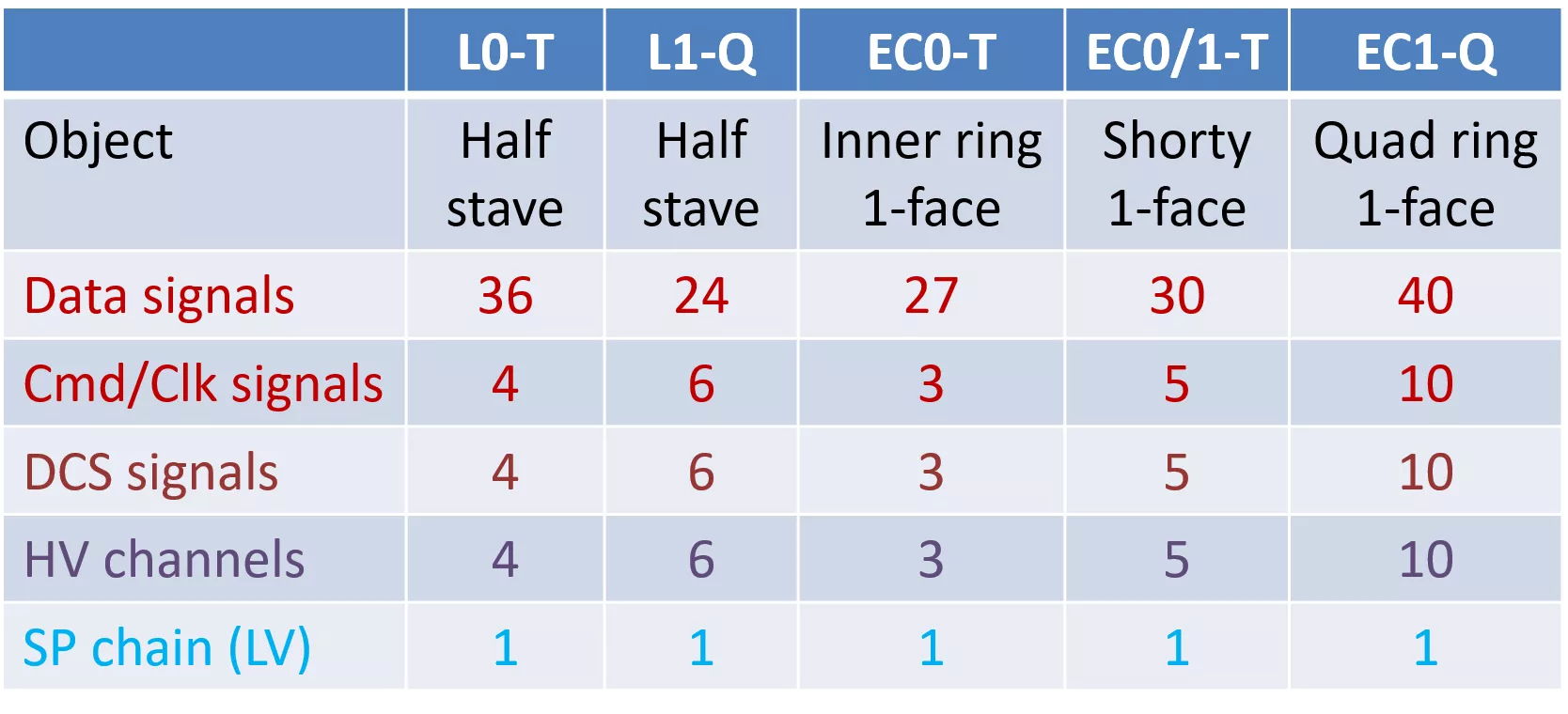
Inner Elex Modularity
•
Half stave and inner ring SP chains:
very inefficient use of 16
DCS chip channels if 1 chip / SP chain
•
Natural (see Q-shell map) combinations sharing same “PP0”:
–
EC Coupled-ring 1-face: inner+outer=3+10 =
13
–
EC Ring 0.5 (Shorty) front+back=5+5 =
10
–
Barrel 3-stave groups: 2*L0+L1=2*4+6 =
14
; L0+2*L1 = 4+2*6 =
16
May/9/2019
2

Current
Opto board
Concept
24
6
Neal’s Table
May/9/2019
3
Quarter-shell Service Channel Map
May/9/2019
4
Unrolled Quarter shell circumference
5
I
m
p
e
d
a
n
c
e
C
a
l
c
u
l
a
t
i
o
n
I
n
n
e
r
P
P
0
First we need to calculate the trace
separation and the thickness of
each layer. We have chosen
.258mm pads with .258mm
separation and layer separation of
0.16764mm, and 1oz of copper.
The cable design and the pad
separation is consistent with a
simple 100ohm differential launch.
6
I
n
t
e
r
n
a
l
l
a
y
e
r
s
7
W
h
y
C
o
p
l
a
n
a
r
W
a
v
e
g
u
i
d
e
?
To improve the
coupling between
differential signals we
will pour copper and
create a Coplanar
waveguide structure to
achieve isolation
~>60dB isolation.
Terminating field line
in a known distance
thus, minimizing stray
inductance and
capacitance.
Good matching between twinax width (1.12mm) and PP0 signal pair spacing (1.25mm)
PP0 termination 12 twinax (Inner barrel case) per row implies PP0 width ~1.6cm
8
N
e
w
T
e
s
t
e
r
b
o
a
r
d
DCS
LV
1.6cm
TwinAx Solder
pads
4 x Type-0
6 cm apart
LV/HV
Type-0
L
0
-
T
Cable
Strain-relief
SLAC is designing two new boards.
The board to the right is being fabricated
now and can be sent to other institutions
with cable attached. The cost is ~$200
dollars fabricated and loaded with a cable.
The board on the bottom is in layout and will
be able to test flex interfaces and isolation.
The board is currently in layout. This board
will emulate the L0-Triplets. We have left
space for the DCS but we need a pin out of
the device. The goal of this board is to be a
to test FLEX connections with the LPAF and
UMPT (LV/HV) connectors and check
isolation of data and command.
9
B
o
a
r
d
s
t
a
c
k
-
u
p
2
0
L
a
y
e
r
s
f
o
r
L
1
-
Q
u
a
d
10
M
o
l
e
x
c
a
b
l
e
P
A
D
S
Drain wire connection
Twinax launch .258x1mm
Size of the pads was chosen to match to the 100 ohm trace.
34AWG is 160um wide but, with the board stack-up and dielectric
material, trace width is 258um.
11
B
o
a
r
d
L
o
s
s
a
n
d
m
a
t
c
h
s
i
m
u
l
a
t
i
o
n
s
f
o
r
2
0
c
m
t
r
a
c
e
o
n
t
h
e
t
o
p
l
a
y
e
r
Evan Van De Wall will present the full chain simulation next week, rough
numbers -17dB from module to Optobox. We need to simulate the eye diagram.
12
I
n
n
e
r
P
P
0
S
t
a
c
k
-
u
p
•
Each row of data and Command with need a layer to run
the traces.
•
Each signal layer needs to have either a ground or a
power supply above or below. (microstrip or stripline
configuration)
•
Does the drain wire need to have a DC return or a RF
connection to ground ?
•
Separation of rows need to be ~5mm for bend radius and
routing of the signals.
Thus min layer 20 layers ~3.7mm thick board.
13
S
t
r
a
i
n
R
e
l
i
e
f
100 Twinax can be bundled with honeycomb strain relief of
15.6mm wide x 7.2mm high
14
C
a
b
l
e
s
t
a
c
k
i
n
g
c
o
n
t
i
n
u
e
15
P
P
0
Q
U
A
D
LPAF/LPAM
FLEX connections
10 rows Twinax
Connections
UMPT/UMPS
LV/HVconnections
2 DCS
Chip
packaged
10x10mm
SLH for DCS
6.5mm for 20
Connections
2mm stack
height
Strain
Relief
(see next
slides)
Still missing Type 0 connections
Board dimensions 1.6cm (width) x 21cm (length) x 3.7mm (thickness)
16
C
o
n
n
e
c
t
o
r
s
Stack height is 5mm.
All connectors
compatible with each
other
Neals Table Local Support Structure for Twinax Data and CMD, Impedance Calculation, Coplanar Waveguides, and New Tester Board - All focusing on industrialization for the SLAC National Accelerator Laboratory.

Download Presentation

Please find below an Image/Link to download the presentation.
The content on the website is provided AS IS for your information and personal use only. It may not be sold, licensed, or shared on other websites without obtaining consent from the author.If you encounter any issues during the download, it is possible that the publisher has removed the file from their server.
You are allowed to download the files provided on this website for personal or commercial use, subject to the condition that they are used lawfully. All files are the property of their respective owners.
The content on the website is provided AS IS for your information and personal use only. It may not be sold, licensed, or shared on other websites without obtaining consent from the author.
E N D
Presentation Transcript
PPO Twinax inputs for industriallization June 3 2019 - SLAC National Accelerator Laboratory Andrew Young, Su Dong (* ayoung@slac.stanford.edu)
Inner Elex Modularity L0-T L1-Q EC0-T EC0/1-T EC1-Q Current Opto board Concept 24 Object Half stave Half stave Inner ring 1-face Shorty 1-face Quad ring 1-face Data signals 36 24 27 30 40 6 Cmd/Clk signals 4 6 3 5 10 DCS signals 4 6 3 5 10 HV channels 4 6 3 5 10 SP chain (LV) 1 1 1 1 1 Half stave and inner ring SP chains: very inefficient use of 16 DCS chip channels if 1 chip / SP chain Natural (see Q-shell map) combinations sharing same PP0 : EC Coupled-ring 1-face: inner+outer=3+10 = 13 EC Ring 0.5 (Shorty) front+back=5+5 = 10 Barrel 3-stave groups: 2*L0+L1=2*4+6 = 14; L0+2*L1 = 4+2*6 = 16 May/9/2019 2
Neals Table Local Support Structure L0 Stave L1 Stave Coupled Ring L0.5 Int Ring L1 Ring Twinax Data Twinax CMD # Structures # Twinax per 72 24 134 60 80 8 8 80 36 160 70 100 12 26 10 20 10 17 6 7 May/9/2019 3
Quarter-shell Service Channel Map Type-1 bundles: Coupled-Rings R0.5 (shorty) Quad Rings PP0 Cooling pipes Unrolled Quarter shell circumference May/9/2019 4
Impedance Calculation Inner PP0 First we need to calculate the trace separation and the thickness of each layer. We have chosen .258mm pads with .258mm separation and layer separation of 0.16764mm, and 1oz of copper. The cable design and the pad separation is consistent with a simple 100ohm differential launch. 5
Why Coplanar Waveguide? To improve the coupling between differential signals we will pour copper and create a Coplanar waveguide structure to achieve isolation ~>60dB isolation. Terminating field line in a known distance thus, minimizing stray inductance and capacitance. Good matching between twinax width (1.12mm) and PP0 signal pair spacing (1.25mm) PP0 termination 12 twinax (Inner barrel case) per row implies PP0 width ~1.6cm 7
New Tester board SLAC is designing two new boards. The board to the right is being fabricated now and can be sent to other institutions with cable attached. The cost is ~$200 dollars fabricated and loaded with a cable. The board on the bottom is in layout and will be able to test flex interfaces and isolation. The board is currently in layout. This board will emulate the L0-Triplets. We have left space for the DCS but we need a pin out of the device. The goal of this board is to be a to test FLEX connections with the LPAF and UMPT (LV/HV) connectors and check isolation of data and command. Cable Strain-relief TwinAx Solder pads 4 x Type-0 6 cm apart L0-T Type-0 LV LV/HV 1.6cm DCS 8
Molex cable PADS Drain wire connection Twinax launch .258x1mm Size of the pads was chosen to match to the 100 ohm trace. 34AWG is 160um wide but, with the board stack-up and dielectric material, trace width is 258um. 10
Board Loss and match simulations for 20cm trace on the top layer Evan Van De Wall will present the full chain simulation next week, rough numbers -17dB from module to Optobox. We need to simulate the eye diagram. 11
Inner PP0 Stack-up Each row of data and Command with need a layer to run the traces. Each signal layer needs to have either a ground or a power supply above or below. (microstrip or stripline configuration) Does the drain wire need to have a DC return or a RF connection to ground ? Separation of rows need to be ~5mm for bend radius and routing of the signals. Thus min layer 20 layers ~3.7mm thick board. 12
Strain Relief 100 Twinax can be bundled with honeycomb strain relief of 15.6mm wide x 7.2mm high 13
PP0 QUAD 2 DCS Chip packaged 10x10mm 10 rows Twinax Connections LPAF/LPAM FLEX connections SLH for DCS 6.5mm for 20 Connections 2mm stack height UMPT/UMPS LV/HVconnections Strain Relief (see next slides) Board dimensions 1.6cm (width) x 21cm (length) x 3.7mm (thickness) Still missing Type 0 connections 15
Connectors Stack height is 5mm. All connectors compatible with each other 16