EIC Silicon Consortium
EIC Silicon Consortium (EICSC) is aiming to develop a MAPS sensor for silicon tracking in an EIC detector, building on collaborations with CERN and other institutions. The consortium's goals include designing new sensors and infrastructure for improved detector solutions. They are actively involved in ongoing R&D efforts to enhance tracking capabilities for particle detection.

Download Presentation

Please find below an Image/Link to download the presentation.
The content on the website is provided AS IS for your information and personal use only. It may not be sold, licensed, or shared on other websites without obtaining consent from the author.If you encounter any issues during the download, it is possible that the publisher has removed the file from their server.
You are allowed to download the files provided on this website for personal or commercial use, subject to the condition that they are used lawfully. All files are the property of their respective owners.
The content on the website is provided AS IS for your information and personal use only. It may not be sold, licensed, or shared on other websites without obtaining consent from the author.
E N D
Presentation Transcript
EIC Silicon Consortium Genesis Membership Current Status Plans 2021_03_16_RNC_EIC_group_meeting - LG 1
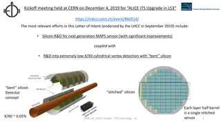
EICSC Genesis ALICE had been working on a next generation thinned and bent MAPs concept for 2018-2019. The initial specifications looked very good and had possible application outside of ALICE. The ALICE conceptual development culminated in an LOI that was endorsed by the LHCC at CERN. This led to a kickoff meeting at CERN for the ITS-3 detector development (December 4, 2019). Unlike previous CERN based sensor development projects the ITS-3 sensor project would welcome outside institutions and consortiums as collaborators in the chip design and would make an agreement to share the IP that is to come from this effort. The specifications for the sensor were had significant overlap with the needs of the EIC. It was proposed to form an EIC Silicon Consortium to work on adopting this sensor at the December 12-13, 2019 EICYR meeting at MIT https://indico.jlab.org/event/348/sessions/1224/attachments/4665/5789/open-mic.pdf 2021_03_16_RNC_EIC_group_meeting - LG 2
Report from the ITS3 kickoff meeting Dec. 4, 2019 CERN Full set of talks at INDICO site: https://indico.cern.ch/event/860914/ Main Effort 2021_03_16_RNC_EIC_group_meeting - LG 3
New sensor design compared to existing ALPIDE 2021_03_16_RNC_EIC_group_meeting - LG 4
EICSC Goals EICSC Goals from the response to the Call for Expressions of Interest for Potential Cooperation on the EIC Experimental Program - November 2, 2020 The goal of this consortium is to develop a MAPS sensor and associated powering, support structures, control and ancillary parts as necessary to produce a detector solution for silicon tracking for the central tracking parts of an EIC detector. The members of this consortium believe that the most successful path to achieve this goal is to join the ongoing effort at CERN to develop a new MAPS sensor based on the Tower-Jazz 65 nm process for use in the upcoming ALICE ITS3 upgrade. The requirements for the ITS3 and what is needed for an EIC tracking sensor have very broad overlap and the synergies of joining an already funded effort strongly increase the probabilities of success. A more detailed description of the current path that leads to an EIC optimized sensor and associated infrastructure can be found in the ERD-25 proposal, https://wiki.bnl.gov/conferences/images/6/6d/ERD25-Report-FY21Proposal-Jun20.pdf 2021_03_16_RNC_EIC_group_meeting - LG 5
Membership and Fitting into the EIC R&D efforts Selected EIC R&D efforts ERD-16 LBNL initiated proposal to use ITS-3 based sensor Detector Collaborati ons ERD-25 EICSC ERD-18 Forming of EICSC Simulations initially performed using a 20 um^2 pixel size sensor with ITS-2 like characteristics (no such sensor exists) ERD-25 formed after January 24, 2020 EIC Detector R&D meeting. https://wiki.bnl.gov/conferences/images/a/a5/EIC_Review_2020-Jan.pdf ERD-25 transitioning into EICEC for R&D purposes in March 2021. EICSC Members: LBNL, BNL instrumentation division, UK collaboration (currently University of Birmingham, RAL, Brunel University - London), JLAB, ORNL, CCNU Wuhan, Groups from INFN (currently Bari, Trieste), Institute of Modern Physics (IMP, China). We have been contacted by other groups expressing interest in working together but as yet EIC Silicon Consortium membership has not been formalized. 2021_03_16_RNC_EIC_group_meeting - LG 6
EICSC need Tracking / Sensor requirements: Currently only MAPS meet this requirement. The newly defined size of the beam pipe shows the need for the sensor pixel size to be < 20 um to meet central tracking requirements. Other sensor candidates either can not be modified to meet the requirements or do not appear to have sufficient support to be available by the time needed. The path of using synergy with the CERN ITS3 effort is, in my opinion, the best path to success. The EICSC goal of developing a full detector solution using sensors based on the ITS3 design is a critical and time sensitive effort for tracking at the EIC 2021_03_16_RNC_EIC_group_meeting - LG 7
Yellow Report driven detector concepts As part of the YR exercise, detector concepts were developed and optimized for EIC tracking. These concepts drive the direction that is needed to move forward in sensor and detector development to realize these concepts. Conceptual layouts are presented below Vertexing inner layers are based on the ITS3 development at CERN BUT the length of the inner staves and the diameters at which these layers sit are markedly different from the ITS3 base design ITS3 length = 30 cm. This is set by the length of stitched sensors on a 12 wafer. EIC length (hybrid) = 42 cm ITS3 radii = 18 mm, 24 mm, 30 mm these radii are set by the integer width of rows of stitched sensors. EIC radii = 36.4 mm and 44.5 mm EIC strawman design (modification of ITS3) Reach larger radii by using 3 bent sections Services exit from both sides of inner layers Engineering work needs to begin Services exit from one end 2021_03_16_RNC_EIC_group_meeting - LG 8
Yellow Report driven detector concepts Staves and discs will be based on a forked EIC specific sensor design based on the ITS3 sensor. The primary concern is yield for long rows of stitched sensors. The plan is to assess yield in the first engineering run and adjust the EIC sensors to optimize yield for the number of stitched sensors in a row. Staves Use shorter lengths of stitched sensors to form staves. Power and signal will need to be propagated along the stave with flex PCBs over the stave length. DC-DC converter? Flex PCB for power/signal Power/signal exit Stitched sensors Stave support structure Discs - could be formed with overlapping staves that conform to the disc diameters or with sensors mounted to half- disc low mass plates. For both of these solutions we will need to optimize the stitched sensor layout on the wafers to provide the right number of stitched sensor lengths to give the proper needed lengths for each stave/disc. This needs study and optimization. 2021_03_16_RNC_EIC_group_meeting - LG 9
Current Status The RAL contribution to MLR1 is the LVDS receiver and CML line driver for use in the digital output stage of the final sensor Contributed to the first ITS-3 MLR submission with RAL. Negotiations underway for access to the process design kit and framework IP sharing agreement for the other chip design institutions (BNL, LBNL). This will allow significantly more sensor design effort from EICSC. In process of gathering proposals for task work in the coming year as we need to engage fully with the ITS3 work packages. Engaging with EIC management at BNL for R&D funding (project and general). Latest EICSC meeting presentations can be found at https://drive.google.com/drive/folders/1vHzNspd6sjdDTsvOOY0AntAkASeeXgZo?usp=sharing 2021_03_16_RNC_EIC_group_meeting - LG 10
Plans (strongly tied to ITS-3 schedule) 2021 Testing and characterization of MLR1 Sensor design for MLR2 or ER R&D into powering, stave/disc construction, cooling, overall infrastructure MLR2 submission 2022 - Testing and characterization of MLR2 Sensor design for ER R&D + prototyping into powering, stave/disc construction, cooling, overall infrastructure ER submission 2023 - Testing and characterization of ITS3 ER and assessment of yield Assessment and planning for EIC sensor fork of ITS3 design Fork off sensor design and work on EIC variant for staves and discs (may move to next year depending on results) Detailed prototyping into powering, stave/disc construction, cooling, overall infrastructure ER submission for EIC variant sensor for staves and discs (may move to next year depending on results) Investigation of adaptation of ITS3 design for use in EIC inner layers (different radii, # layers, services from both ends to meet length requirements, etc. 2024 Testing and characterization of EIC ER and assessment of yield Si design for EIC ER2 Detailed prototyping into powering, stave/disc construction, cooling, overall infrastructure using EIC ER1 prototypes. ER2 submission for EIC variant sensor for staves and discs adaptation of ITS3 design for use in EIC inner layers and integration of design into ER2 if necessary. We are developing two detector concepts: 1. ITS3 like for the vertexing layers. 2. EIC variant for the staves and discs. We will need to develop the capabilities to bring both detector concepts and the associated infrastructure to completion. 2021_03_16_RNC_EIC_group_meeting - LG 11
Backup 2021_03_16_RNC_EIC_group_meeting - LG 12
Expanded task list for 2021 (applies to following years as well) These tasks compliment and are in addition to robust participation in the ITS3 work packages to prepare for the EIC vertexing layers design. 2021 Testing and characterization of MLR1 design of testing system that extends into the testing of the next submissions. Beam testing, Latch-up testing, SEU testing, radiation tolerance testing (kRAD, NIEL), firmware, software, mechanical carriers, alignment stations, analysis, etc. This work is starting in ITS3, we can/should join this effort. Sensor design for MLR2 or ER Inclusion of other silicon design sites into the design process (in progress), Assessment of the testing results and incorporation into the new designs, significant digital design (in pixel logic, readout structures and architecture), design for stitching, significantly more complex structures and pixel layout studies, design for yield, etc. R&D into powering, stave/disc construction, cooling, overall infrastructure Take up DC-DC converter and serial powering R&D, studies of stave and disc design, cooling studies (air for inner layers, liquid? For outer layers and discs), investigation of on detector data multiplexing and implications for single point failure and redundancy studies, initial studies for carbon fiber designs for overall mechanical support structures, services routing studies, radiation length minimization, etc. MLR2 submission Detailed silicon design as per sensor design section, layout and DRC, integration into MLR, etc. 2021_02_04 EICSC meeting - LG 13
Sensor development milestones 2021_03_16_RNC_EIC_group_meeting - LG 14
Organization of effort ITS3-WP1: Physics studies, Simulation and Reconstruction Physics performance studies Detector functional requirements Detector model and simulation Reconstruction alice-its3-wp1@cern.ch ITS3-WP2: Pixel chip design Test structures and validation of the technology Optimization of the pixel layout Large area building block prototypes Full scale prototypes Final chip ITS3-WP3: Pixel chip characterization Development of hardware and software for the pixel chip characterization Laboratory, Beam and Radiation tests Pixel chip device simulation alice-its3-wp2@cern.ch alice-its3-wp3@cern.ch 2021_03_16_RNC_EIC_group_meeting - LG 15
Organization of effort ITS3-WP4: Pixel sensor thinning, bending and interconnection Tests with existing material (ALPIDE wafers) Tests with 300 mm dummy wafers Test with full-scale prototypes Mechanical, electrical and functional validation of the procedures alice-its3-wp4@cern.ch ITS3-WP5: Mechanics and cooling Selection and characterization of carbon materials (structural and thermal properties) Development and production of support structures Development, production and validation of the Engineering Module based on dummy chips Development, production and validation of the Qualification Module based on prototype chips Production of the Final Module based on final chips alice-its3-wp5@cern.ch 2021_03_16_RNC_EIC_group_meeting - LG 16
Group Efforts in this development We are joining the sensor R&D effort to optimize the sensor characteristics (to the extent that they are not already) for use at the EIC. We will soon be selecting work packages to join officially but expect to the active in WP2, WP3 with lesser directed efforts in WP4, WP5. It is hoped that this effort should have significant overlap with the EIC efforts in the infrastructure of building of the silicon tracking detectors. 2021_03_16_RNC_EIC_group_meeting - LG 17


")