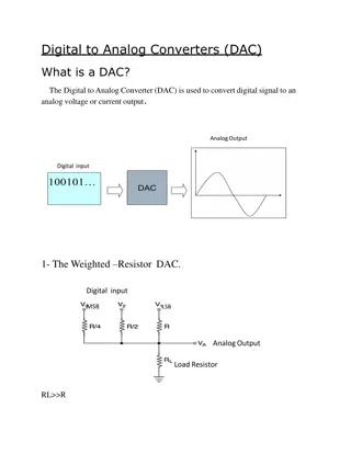
Digital to Analog Converters
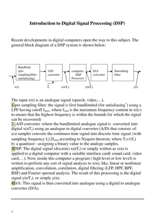
Digital-to-Analog Converters (DACs) play a crucial role in converting digital data to analog signals. Explore DAC applications, performance parameters, potential errors like quantization error and non-linearity, and DAC architectures such as R-2-R ladder and Switched Capacitors. Understand the importance of monotonicity, resistor strings, and clock synchronization for optimal DAC functionality.

Download Presentation

Please find below an Image/Link to download the presentation.
The content on the website is provided AS IS for your information and personal use only. It may not be sold, licensed, or shared on other websites without obtaining consent from the author.If you encounter any issues during the download, it is possible that the publisher has removed the file from their server.
You are allowed to download the files provided on this website for personal or commercial use, subject to the condition that they are used lawfully. All files are the property of their respective owners.
The content on the website is provided AS IS for your information and personal use only. It may not be sold, licensed, or shared on other websites without obtaining consent from the author.
E N D
Presentation Transcript
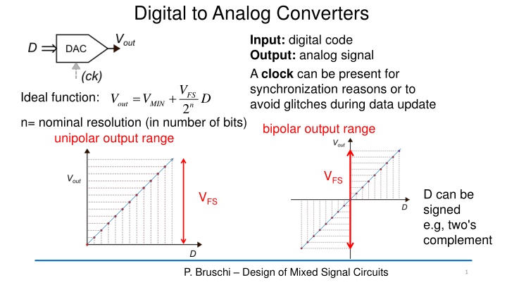
Digital to Analog Converters Input: digital code Output: analog signal A clock can be present for synchronization reasons or to avoid glitches during data update V = + Ideal function: FS n V V D out MIN 2 n= nominal resolution (in number of bits) bipolar output range unipolar output range VFS D can be signed e.g, two's complement VFS P. Bruschi Design of Mixed Signal Circuits 1
DAC applications Digital to analog signal reconstruction: e.g. audio and video signals, actuator control (e.g. control of motors, solenoids, piezoactuators Sensor excitation: generation of bias voltages, sinusoidal waveforms, etc) Direct Digital Synthesis (DDS) of waveforms for telecommunications Trimming of analog blocks (e.g. offset nulling) Feedback components in ADCs P. Bruschi Design of Mixed Signal Circuits 2
DAC performance parameters DAC errors Quantization error Offset Gain Non-linearity INL DNL Noise Energy of the glitches (nV s) DAC speed: settling time, sample per seconds (sps), Maximum output current Power consumption P. Bruschi Design of Mixed Signal Circuits 3
INL, DNL Ideal case (absence of non-linearity errors) V LSB = FS n 2 real case INL LSB LSB = = ( ) k DNL Unit LSB k LSB |DNL|> 1 LSB: non-monotonicity P. Bruschi Design of Mixed Signal Circuits 4
DAC Architectures Pros Cons Potentially non-monotonic Suffer from the on-resistance of the switches Reduced number of resistor of similar value R-2-R ladder Guaranteed monotonic Low power consumption Very large number of resistors Resistor String Very fast. No need for resistors. Can be designed to be always monotonic Current output. Flicker Noise Current Steering The output may be not available in the whole clock cycle. Large glitches Optimal power vs speed trade-off Switched Capacitors P. Bruschi Design of Mixed Signal Circuits 5
DAC resistor string For any value of code D, only one switch at a time is on, selecting one of the 2nvoltage levels produced by the resistive divider n 2 resistors 2 switches If code D turns on a certain switch, code D+1 turns on the switch placed un position up, then the output voltage can only grow n The monotonicity is guaranteed Digital decoder n n 2 P. Bruschi Design of Mixed Signal Circuits 6
INL in a resistor string: a simple estimate We consider a code that, in the ideal case, select the mid voltage: Ideally 1 2 R R = V = out id V REF 2 R R = + = , R R R R In a real case: 1 2 2 2 R + R V R + R R 2 = = ref = + V V 1 1 out ref 2 R R R 2 2 1 2 V R R ref = V V n R R 2 V LSB R R = INL ref = 2 2n INL 2 2 2 2 V ref R + V = LSB = V V 1 REF n out ref R R 2 1 2 P. Bruschi Design of Mixed Signal Circuits 7
INL and resistor matching In an n-bit DAC, to have an |INL|<1 LSB, the relative matching errors should be: V LSB R = 2 2n INL R 1 R R R R 2 n 2 1 2 2n Example: 16 bit DAC: 1 2 R Example: 12 bit DAC: R 1 R R 6 10 5 3 10 14 10 2 Unfeasible. Requires complicated post-production trimming Feasible, with large area occupation P. Bruschi Design of Mixed Signal Circuits 8
Current Steering DAC The current of mosfets that are not routed to the output (their bit is 0), is not interrupted but is routed to a constant voltage (Vk) to keep the mosfet ready to be connected to the output in a short time I0 2I0 I I I I = = REF n 2k = = k I I b 2 b D REF n REF n 0 = 2 0 out k 2k k D b 2 2 k It can be made monotonic-guaranteed by driving the 2nmosfets of the array with thermometric coding It suffers from the same INL problem of the resistor string DAC P. Bruschi Design of Mixed Signal Circuits 9
Thermometric coding thermometric coding D 2nidentical current sources I=I0 randomly placed into the matrix D devices of the matrix are routed to the output The first D lines are set to 1 If D is incremented by one, one more device is routed to the output: Iout increases. Monotonicity is guaranteed 2ndevices (always in parallel) 2ndevices P. Bruschi Design of Mixed Signal Circuits 10
Analog to Digital Converters (ADCs) The characteristic of an n-bit ADC with no offset, gain, and non-linearity errors (only quantization errors) It is useful to refer to the equivalent voltage of D V LSB = + FS n in dig v V D MIN 2 V = FS 2 LSB vin-digmust be the best approximation of vin, given the number of bit of D n P. Bruschi Design of Mixed Signal Circuits 11
Nyquist - Rate and oversampling ADCs The output code depends only on the last conversion. Previous conversions do not affect the present code 2 f B Nyquist Rate ADC: S S The output code depends also on the previous history of sampled data. 2 f B Oversampling ADC: S S P. Bruschi Design of Mixed Signal Circuits 12
Nyquist rate ADCs Counting ADCs Successive Approximation (binary search) ADCs Flash ADCs (pure flash or sub-ranging flash) Double-Slope ADCs Model that can represent most Nyquist rate ADC types, with the exception of single and double-slope ADCs In Nyquist-rate ADCs, the INL and DNL are mainly due to the DAC feedback P. Bruschi Design of Mixed Signal Circuits 13
A very common SAR ADC: the charge-redistribution ADC preamplified comparator capacitive DAC = = 2k C C C C 0 k 0 A 1 1 n n ( ) + + = = = + = k n n 2 2 1 2 C C C C C C C C 0 0 0 0 0 tot A k = = 0 0 k k P. Bruschi Design of Mixed Signal Circuits 14
Reset phase The op-amp is closed in unity gain -vn analog input signal Vin 0 All capacitors are in parallel, with one terminal connected to the input voltage Vin. P. Bruschi Design of Mixed Signal Circuits 15
Sampling phase The op-amp is placed in open loop configuration and the bottom plates of all capacitors are connected to gnd. The voltage of the top plates (Vtop) is free to evolve (it is floating, no current comes from the OP to Vtop) P. Bruschi Design of Mixed Signal Circuits 16
Top voltage in the sampling phase nv v V n in V The voltage on Ctot does not change Reset in Sampling ( ) s t ( ) s = V V top = ( in V Ctot V t 0) ( ) s V v t nv top in n P. Bruschi Design of Mixed Signal Circuits 17
SAR phases composite comparator = kb Sequence: SARn-1...... SAR0 Phase SARkbegins by connecting the bottom plate of Ckto the reference voltage VREFthrough switch Sk This causes a jump in voltage Vtop. Bit k-th is the output of the composite comparator (Vb) at the end of phase SARk If bk=0 Skcomes back to gnd, else it remains at VREF Phase SARk P. Bruschi Design of Mixed Signal Circuits 18
Composite comparator VoA=A(ViA vn) Vtop ViA The gain of OA is so large that the offset and hysteresis of CMP has negligible impact on the composite comparator characteristics. 1 if 0 if v Vb V V v v iA n = V = V V b iA top iA n 1 if V v V top n top n = V b 0 if V v V v top n top n P. Bruschi Design of Mixed Signal Circuits 19
Phase SARk: calculation of the Vtopjump Vtopat phase SARk All-capacitor network: equivalent circuit for variations. Capacitors can be replaced by a resistors of value 1/C k C 2 2 C C = = = 0 V k V V VC REF top k n 0 tot V = = V REF n = 2k V V LSB 2 k LSB P. Bruschi Design of Mixed Signal Circuits 20
Phase SARn-1 Vb V V = = = 1 1 n n 2 2 V V REF n REF 1 n LSB 2 2 from sampling phase V ( ) s t ( ) s ( ) s t ( ) s = + = + V V v t V V v t REF 1 top in n n in n 2 Decision for bit bn-1(taken at time tn-1= end of phase SARn-1) V ( ) ( ) ( ) s t ( ) s ( ) = + 1 if V V t v t V v t v t REF 1 1 b top n n n 1 in n n n 2 P. Bruschi Design of Mixed Signal Circuits 21
Phase SARn-1 V + possible values of Vin(ts) and resulting value of bn-1 ( ) s t ( ) s ( ) nb = 1 if: V v t v t REF 1 1 in n n n 2 V ( ) s t ( ) s ( ) + V v t v t REF 1 in n n n 2 bn-1=1 Subtraction of two noise samples taken at different times: constant and correlated components are rejected (CDS). bn-1=0 Neglecting noise / offset components, the condition becomes: ( ) in s V t This is in conformity with the successive approximation algorithm V REF 2 P. Bruschi Design of Mixed Signal Circuits 22
Phase SARn-2 Vb V V = = 1 n V REF 2 n 2 4 Switch Sn-1goes back to gnd if bn-1=0 Otherwise, it remains to VREF Decision : bit bn-2=1 if: ( ) s t ( ) s ( ) = + + V V v t b V V v t 1 1 2 top in n n n n 2 n n If Sn-1comes back to gnd, it subtracts Vn-1from Vtop P. Bruschi Design of Mixed Signal Circuits 23
Decision for bn-2 ( ) s t = + 1 if: b V b V V 2 1 1 2 n in n n n Vtst(n 2) bn-2=1 bn-2=0 if bn-1=1 Vtst(n 2)= bn-2=1 bn-2=0 if bn-1=0 Vtst(n 2)= P. Bruschi Design of Mixed Signal Circuits 24
Generalization At k-th step (phase SARk) , bit bkis determined from the comparison of Vin( ts) with: = + + + + ( ) k .... V b V b V b V V At any step the increment is halved + + 1 1 2 2 1 1 tst n n n n k k k Increments applied in previous phases and maintained only if the corresponding bits are 1 V = + 1 k V k 2 At the last phase, SAR0, the LSB (b0) is determined and the conversion is complete. The bits determined in the successive phases are stored inside a register of the control logic and can be retrieved at the end of conversion. P. Bruschi Design of Mixed Signal Circuits 25
Examples of conversion cycle bn-1= 1 bn-2= 0 V V V = + REF REF REF 8 4 8 P. Bruschi Design of Mixed Signal Circuits 26


")