Custom Design Flow for Layout and Simulation
 undefined
E
x
t
r
a
c
t
i
o
n
,
L
V
S
a
n
d
P
o
s
t
-
l
a
y
o
u
t
s
i
m
u
l
a
t
i
o
n
Dr Basel Halak
C
u
s
t
o
m
D
e
s
i
g
n
F
l
o
w
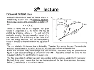
Specification
Schematic
design
Simulation
Meets
the spec?
yes
no
Layout design
DRC
LVS
Parasitic Extraction
Simulation
Meets the
spec?
Completed design
no
LVS Checking
DRC Checking
L
e
a
r
n
i
n
g
O
u
t
c
o
m
e
s
A
f
t
e
r
c
o
m
p
l
e
t
i
n
g
t
h
i
s
u
n
i
t
,
y
o
u
s
h
o
u
l
d
b
e
a
b
l
e
t
o
:
U
s
e
l
a
y
o
u
t
v
e
r
s
u
s
s
c
h
e
m
a
t
i
c
(
L
V
S
)
t
o
o
l
s
P
e
r
f
o
r
m
a
n
e
x
t
r
a
c
t
i
o
n
w
i
t
h
p
a
r
a
s
i
t
i
c
e
l
e
m
e
n
t
s
U
s
e
t
h
e
h
i
e
r
a
r
c
h
y
e
d
i
t
o
r
R
u
n
a
p
o
s
t
-
l
a
y
o
u
t
s
i
m
u
l
a
t
i
o
n
L
e
a
r
n
i
n
g
O
u
t
c
o
m
e
s
A
f
t
e
r
c
o
m
p
l
e
t
i
n
g
t
h
i
s
u
n
i
t
,
y
o
u
s
h
o
u
l
d
b
e
a
b
l
e
t
o
:
U
s
e
l
a
y
o
u
t
v
e
r
s
u
s
s
c
h
e
m
a
t
i
c
(
L
V
S
)
t
o
o
l
s
P
e
r
f
o
r
m
a
n
e
x
t
r
a
c
t
i
o
n
w
i
t
h
p
a
r
a
s
i
t
i
c
e
l
e
m
e
n
t
s
U
s
e
t
h
e
h
i
e
r
a
r
c
h
y
e
d
i
t
o
r
R
u
n
a
p
o
s
t
-
l
a
y
o
u
t
s
i
m
u
l
a
t
i
o
n
W
h
e
r
e
w
e
l
e
f
t
o
f
f
I
n
t
h
e
l
a
s
t
l
e
c
t
u
r
e
,
y
o
u
s
a
w
h
o
w
t
o
u
s
e
V
i
r
t
u
o
s
o
t
o
c
r
e
a
t
e
a
b
a
s
i
c
l
a
y
o
u
t
c
e
l
l
.
Y
o
u
r
l
a
y
o
u
t
m
u
c
h
b
e
f
r
e
e
f
r
o
m
a
l
l
D
R
C
e
r
r
o
r
s
b
e
f
o
r
e
y
o
u
d
o
L
V
S
c
h
e
c
k
i
n
g
E
x
t
r
a
c
t
i
o
n
T
h
e
e
x
t
r
a
c
t
i
o
n
t
o
o
l
i
s
i
n
v
o
k
e
d
f
r
o
m
w
i
t
h
i
n
t
h
e
L
a
y
o
u
t
w
i
n
d
o
w
T
h
i
s
b
r
i
n
g
u
p
t
h
e
e
x
t
r
a
c
t
f
o
r
m
(
R
u
n
A
s
s
u
r
a
L
V
S
)
L
a
y
o
u
t
v
e
r
s
u
s
s
c
h
e
m
a
t
i
c
(
L
V
S
)
L
a
y
o
u
t
v
e
r
s
u
s
s
c
h
e
m
a
t
i
c
c
o
m
p
a
r
e
s
t
h
e
e
x
t
r
a
c
t
e
d
n
e
t
l
i
s
t
t
o
t
h
e
s
c
h
e
m
a
t
i
c
Y
o
u
c
a
n
i
n
v
o
k
e
t
h
e
L
V
S
t
o
o
l
f
r
o
m
t
h
e
L
a
y
o
u
t
v
i
e
w
w
i
n
d
o
w
L
a
y
o
u
t
v
e
r
s
u
s
s
c
h
e
m
a
t
i
c
(
L
V
S
)
H
e
r
e
w
e
w
i
l
l
p
e
r
f
o
r
m
t
h
e
c
i
r
c
u
i
t
e
x
t
r
a
c
t
i
o
n
,
t
h
a
t
i
s
,
a
l
l
t
h
e
p
a
r
a
s
i
t
i
c
s
r
e
s
u
l
t
i
n
g
t
h
e
l
a
y
o
u
t
o
f
t
h
e
d
e
v
i
c
e
s
(
c
a
p
a
c
i
t
a
n
c
e
s
,
d
i
o
d
e
s
,
a
n
d
o
t
h
e
r
c
o
m
p
o
n
e
n
t
s
t
h
a
t
c
a
n
e
x
i
s
t
d
u
e
t
o
t
h
e
i
n
t
e
r
a
c
t
i
o
n
b
e
t
w
e
e
n
d
i
f
f
e
r
e
n
t
l
a
y
e
r
s
)
.
T
h
e
l
a
y
o
u
t
v
i
e
w
w
i
l
l
a
l
s
o
b
e
c
o
m
p
a
r
e
d
w
i
t
h
t
h
e
s
c
h
e
m
a
t
i
c
(
L
a
y
o
u
t
v
e
r
s
u
s
S
c
h
e
m
a
t
i
c
,
o
r
s
i
m
p
l
y
L
V
S
)
W
i
t
h
o
u
t
a
n
y
D
R
C
e
r
r
o
r
,
s
e
l
e
c
t
A
s
s
u
r
a
→
R
u
n
L
V
S
.
I
n
t
h
e
m
a
i
n
f
o
r
m
p
r
e
s
s
S
e
t
S
w
i
t
c
h
e
s
,
s
e
l
e
c
t
t
h
e
r
e
s
i
m
u
l
a
t
e
_
e
x
t
r
a
c
t
e
d
o
p
t
i
o
n
a
n
d
p
r
e
s
s
O
K
.
T
h
i
s
e
n
s
u
r
e
s
t
h
e
u
s
e
o
f
t
h
i
s
L
V
S
r
u
n
f
o
r
R
C
X
.
R
u
n
n
i
n
g
t
h
e
L
V
S
c
h
e
c
k
I
n
t
h
e
R
U
N
A
s
s
u
r
a
L
V
S
w
i
n
d
o
w
:
1.
The Cell name should be the same as your Run name.
2.
Technology should be chosen by c35b4.
3.
The extract rule should be:
/home/esdcad/designkits/ams/v400/assura/c35b4/c35b4/extract.rul
4.
The Compare rules should be
home/designkits/ams/v400/assura/c35b4/c35b4/compare.rul
5.
The binding files should be
/home/esdcad/designkits/ams/v400/assura/c35b4/c35b4/bind.rul
6.
RSF include should be
/home/esdcad/designkits/ams/v400/assura/c35b4/c35b4/LVSinclude.rsf
7.
S
e
l
e
c
t
t
h
e
s
w
i
t
c
h
e
s
o
p
t
i
o
n
r
e
s
i
m
u
l
a
t
e
_
e
x
t
r
a
c
t
e
d
t
o
e
n
s
u
r
e
e
n
s
u
r
e
s
t
h
e
u
s
e
o
f
t
h
i
s
L
V
S
r
u
n
f
o
r
R
C
X
.
L
a
y
o
u
t
v
e
r
s
u
s
s
c
h
e
m
a
t
i
c
(
L
V
S
)
I
n
t
h
e
m
a
i
n
f
o
r
m
p
r
e
s
s
O
K
t
o
s
t
a
r
t
L
V
S
.
T
h
e
n
y
o
u
w
i
l
l
s
e
e
t
h
e
p
r
o
g
r
e
s
s
w
i
n
d
o
w
.
C
h
e
c
k
i
n
g
t
h
e
L
V
S
o
u
t
p
u
t
I
f
t
h
e
r
e
i
s
n
o
t
h
i
n
g
w
r
o
n
g
,
y
o
u
w
i
l
l
r
e
c
e
i
v
e
t
h
i
s
m
e
s
s
a
g
e
.
L
a
y
o
u
t
v
e
r
s
u
s
s
c
h
e
m
a
t
i
c
(
L
V
S
)
C
l
i
c
k
Y
e
s
.
Y
o
u
w
i
l
l
s
e
e
t
h
e
S
c
h
e
m
a
t
i
c
a
n
d
L
a
y
o
u
t
M
a
t
c
h
.
T
y
p
i
c
a
l
L
V
S
e
r
r
o
r
s
I
n
o
u
r
c
a
s
e
y
o
u
s
h
o
u
l
d
g
e
t
a
t
l
e
a
s
t
o
n
e
e
r
r
o
r
–
t
h
e
t
e
r
m
i
n
a
l
s
d
o
n
’
t
a
l
l
m
a
t
c
h
R
e
a
d
i
n
g
f
u
r
t
h
e
r
o
n
,
i
t
i
s
c
l
e
a
r
t
h
a
t
t
h
e
p
r
o
b
l
e
m
i
s
w
i
t
h
t
h
e
Z
t
e
r
m
i
n
a
l
i
n
t
h
e
l
a
y
o
u
t
C
l
e
a
r
l
y
,
I
h
a
v
e
l
a
b
e
l
l
e
d
t
h
e
o
u
t
p
u
t
Z
i
n
t
h
e
l
a
y
o
u
t
a
n
d
Y
i
n
t
h
e
s
c
h
e
m
a
t
i
c
–
a
n
e
a
s
y
f
i
x
.
T
y
p
i
c
a
l
L
V
S
e
r
r
o
r
s
S
o
o
f
y
o
u
h
a
v
e
L
V
S
e
r
r
o
r
s
y
o
u
w
i
l
l
r
e
c
e
i
v
e
t
h
e
f
o
l
l
o
w
i
n
g
m
e
s
s
a
g
e
w
h
i
c
h
l
i
s
t
s
a
l
l
e
r
r
o
r
s
.
C
l
i
c
k
o
k
t
o
g
o
t
o
D
e
b
u
g
W
i
n
d
o
w
T
y
p
i
c
a
l
L
V
S
e
r
r
o
r
s
L
V
S
D
e
b
u
g
W
i
n
d
o
w
g
i
v
e
s
m
o
r
e
d
e
t
a
i
l
s
o
n
e
a
c
h
e
r
r
o
r
i
n
t
h
e
s
u
m
m
a
r
y
b
o
x
D
o
u
b
l
e
c
l
i
c
k
t
h
e
P
i
n
s
T
y
p
i
c
a
l
L
V
S
e
r
r
o
r
s
Y
o
u
c
a
n
f
i
n
d
t
h
e
m
i
s
m
a
t
c
h
d
e
t
a
i
l
a
n
d
f
i
x
i
t
.
L
e
a
r
n
i
n
g
O
u
t
c
o
m
e
s
O
u
t
c
o
m
e
s
A
f
t
e
r
c
o
m
p
l
e
t
i
n
g
t
h
i
s
u
n
i
t
,
y
o
u
s
h
o
u
l
d
b
e
a
b
l
e
t
o
:
U
s
e
l
a
y
o
u
t
v
e
r
s
u
s
s
c
h
e
m
a
t
i
c
(
L
V
S
)
t
o
o
l
s
P
e
r
f
o
r
m
a
n
e
x
t
r
a
c
t
i
o
n
w
i
t
h
p
a
r
a
s
i
t
i
c
e
l
e
m
e
n
t
s
U
s
e
t
h
e
h
i
e
r
a
r
c
h
y
e
d
i
t
o
r
R
u
n
a
p
o
s
t
-
l
a
y
o
u
t
s
i
m
u
l
a
t
i
o
n
E
x
t
r
a
c
t
i
o
n
Y
o
u
n
e
e
d
t
o
e
n
s
u
r
e
t
h
a
t
y
o
u
r
d
e
s
i
g
n
i
s
f
r
e
e
f
r
o
m
L
V
S
e
r
r
o
r
s
b
e
f
o
r
e
y
o
u
c
a
n
p
r
o
c
e
e
d
w
i
t
h
t
h
e
e
x
t
r
a
c
t
i
o
n
b
T
h
e
e
x
t
r
a
c
t
i
o
n
t
o
o
l
i
s
i
n
v
o
k
e
d
f
r
o
m
w
i
t
h
i
n
t
h
e
L
a
y
o
u
t
w
i
n
d
o
w
:
a
s
f
o
l
l
o
w
s
:
A
s
s
u
r
a
→
R
u
n
Q
R
C
a
n
d
t
o
c
h
o
o
s
e
E
x
t
r
a
c
t
i
o
n
t
a
b
.
F
o
r
t
h
e
r
e
f
e
r
e
n
c
e
n
o
d
e
(
R
e
f
N
o
d
e
)
w
r
i
t
e
g
n
d
!
.
P
r
o
c
e
e
d
w
i
t
h
O
K
.
S
e
t
u
p
t
a
p
T
h
e
T
e
c
h
n
o
l
o
g
y
i
n
S
e
t
u
p
p
a
g
e
s
h
o
u
l
d
b
e
c
3
5
b
4
.
R
u
l
e
s
e
t
T
y
p
i
c
a
l
O
u
t
p
u
t
s
h
o
u
l
d
b
e
Extracted view
Y
o
u
s
h
o
u
l
d
p
i
c
k
a
g
o
o
d
v
i
e
w
n
a
m
e
t
o
m
a
k
e
i
t
e
a
s
y
t
o
d
i
f
f
e
r
e
n
t
i
a
t
e
b
e
t
w
e
e
n
e
x
t
r
a
c
t
i
o
n
v
e
r
s
i
o
n
s
.
E
x
t
r
a
c
t
i
o
n
T
a
p
E
x
t
r
a
c
t
i
o
n
T
y
p
e
s
h
o
u
l
d
b
e
C
O
n
l
y
,
t
h
e
o
t
h
e
r
o
p
t
i
o
n
s
c
a
n
b
e
u
s
e
d
i
n
f
u
r
t
h
e
r
d
e
v
e
l
o
p
m
e
n
t
.
C
a
p
C
o
u
p
l
i
n
g
M
o
d
e
i
s
C
o
u
p
l
e
d
(
i
.
e
.
i
n
t
o
a
c
c
o
u
n
t
c
o
u
p
l
i
n
g
c
a
p
a
c
i
t
a
n
c
e
s
)
.
R
e
f
N
o
d
e
i
s
g
n
d
!
N
e
t
l
i
s
t
i
n
g
T
a
p
D
e
s
i
g
n
C
a
p
a
c
i
t
o
r
M
o
d
e
l
s
,
P
a
r
a
s
i
t
i
c
C
a
p
a
c
i
t
o
r
M
o
d
e
l
s
,
D
e
s
i
g
n
R
e
s
i
s
t
o
r
M
o
d
e
l
s
a
n
d
P
a
r
a
s
i
t
i
c
R
e
s
i
s
t
o
r
M
o
d
e
l
s
a
r
e
a
l
l
c
h
o
s
e
n
D
o
n
o
t
i
n
c
l
u
d
e
.
R
u
n
t
h
e
e
x
t
r
a
c
t
i
o
n
C
l
i
c
k
O
K
t
o
r
u
n
t
h
e
e
x
t
r
a
c
t
i
o
n
Extraction can take a while on a large circuit
Check for no errors
Errors are rare – typically just ‘check and save’ errors
T
h
e
e
x
t
r
a
c
t
e
d
v
i
e
w
T
h
i
s
h
a
s
c
r
e
a
t
e
d
a
n
e
w
c
e
l
l
v
i
e
w
c
a
l
l
e
d
‘
i
n
v
_
e
x
_
C
_
o
n
l
y
0
2
’
T
h
e
e
x
t
r
a
c
t
e
d
v
i
e
w
L
o
o
k
s
a
b
i
t
l
i
k
e
t
h
e
l
a
y
o
u
t
I
t
i
s
a
l
a
y
o
u
t
v
i
e
w
,
b
u
t
w
i
t
h
e
x
t
r
a
c
t
e
d
d
e
v
i
c
e
s
a
n
d
p
a
r
a
s
i
t
i
c
s
h
o
w
n
E
x
t
r
a
c
t
i
n
g
w
i
t
h
p
a
r
a
s
i
t
i
c
s
T
h
e
e
x
t
r
a
c
t
i
o
n
w
i
l
l
t
a
k
e
l
o
n
g
e
r
t
h
a
n
b
e
f
o
r
e
,
d
u
e
t
o
t
h
e
e
x
t
r
a
r
u
l
e
s
i
t
n
e
e
d
s
t
o
r
u
n
C
h
e
c
k
t
h
e
C
I
W
(
m
a
i
n
I
C
F
B
w
i
n
d
o
w
)
f
o
r
a
n
y
e
r
r
o
r
s
O
p
e
n
t
h
e
e
x
t
r
a
c
t
e
d
v
i
e
w
S
p
o
t
t
h
e
e
x
t
r
a
c
a
p
a
c
i
t
a
n
c
e
s
A
M
S
u
s
e
s
a
l
u
m
p
e
d
m
o
d
e
l
–
i
.
e
.
t
o
t
a
l
c
a
p
a
c
i
t
a
n
c
e
f
r
o
m
o
n
e
n
o
d
e
t
o
a
n
o
t
h
e
r
.
L
e
a
r
n
i
n
g
O
u
t
c
o
m
e
s
O
u
t
c
o
m
e
s
A
f
t
e
r
c
o
m
p
l
e
t
i
n
g
t
h
i
s
u
n
i
t
,
y
o
u
s
h
o
u
l
d
b
e
a
b
l
e
t
o
:
U
s
e
l
a
y
o
u
t
v
e
r
s
u
s
s
c
h
e
m
a
t
i
c
(
L
V
S
)
t
o
o
l
s
P
e
r
f
o
r
m
a
n
e
x
t
r
a
c
t
i
o
n
w
i
t
h
p
a
r
a
s
i
t
i
c
e
l
e
m
e
n
t
s
U
s
e
t
h
e
h
i
e
r
a
r
c
h
y
e
d
i
t
o
r
R
u
n
a
p
o
s
t
-
l
a
y
o
u
t
s
i
m
u
l
a
t
i
o
n
E
x
t
r
a
c
t
i
n
g
w
i
t
h
p
a
r
a
s
i
t
i
c
s
W
e
w
a
n
t
t
o
s
i
m
u
l
a
t
e
t
h
e
p
a
r
a
s
i
t
i
c
c
o
m
p
o
n
e
n
t
s
i
n
t
h
e
l
a
y
o
u
t
t
o
s
e
e
t
h
e
i
r
e
f
f
e
c
t
o
n
t
h
e
p
e
r
f
o
r
m
a
n
c
e
E.g. rise time, fall time
P
a
r
a
s
i
t
i
c
c
o
m
p
o
n
e
n
t
s
c
o
n
s
i
s
t
o
f
R
s
a
n
d
C
s
Resistance of interconnect
Capacitance between layers
T
h
e
A
M
S
k
i
t
a
l
l
o
w
s
u
s
t
o
e
x
t
r
a
c
t
t
h
e
p
a
r
a
s
i
t
i
c
c
a
p
a
c
i
t
a
n
c
e
s
o
n
l
y
P
o
s
t
-
l
a
y
o
u
t
s
i
m
u
l
a
t
i
o
n
T
h
e
s
c
h
e
m
a
t
i
c
y
o
u
h
a
v
e
d
r
a
w
n
i
s
n
o
t
r
e
a
l
i
s
t
i
c
T
h
e
e
x
t
r
a
c
t
e
d
l
a
y
o
u
t
,
c
o
n
t
a
i
n
i
n
g
p
a
r
a
s
i
t
i
c
c
a
p
a
c
i
t
a
n
c
e
s
i
s
f
a
r
m
o
r
e
r
e
a
l
i
s
t
i
c
a
n
d
i
t
i
s
u
s
e
f
u
l
t
o
s
i
m
u
l
a
t
e
t
h
i
s
t
o
i
n
c
r
e
a
s
e
c
o
n
f
i
d
e
n
c
e
i
n
y
o
u
r
d
e
s
i
g
n
F
i
r
s
t
w
e
n
e
e
d
a
t
e
s
t
c
i
r
c
u
i
t
f
o
r
o
u
r
i
n
v
e
r
t
e
r
,
t
h
e
n
w
e
n
e
e
d
t
o
t
e
l
l
t
h
e
s
i
m
u
l
a
t
o
r
t
o
u
s
e
t
h
e
e
x
t
r
a
c
t
e
d
v
i
e
w
,
n
o
t
t
h
e
s
c
h
e
m
a
t
i
c
v
i
e
w
P
o
s
t
-
l
a
y
o
u
t
s
i
m
u
l
a
t
i
o
n
1.
For this simulation you need to use the inverter cell which
has the following views (schematic, layout, extracted and
symbol)
2.
Create a new test schematic called
Test_Inverter_layout
as shown below using your fixed dimension inverter in it
H
o
w
t
o
u
s
e
t
h
e
H
i
e
r
a
r
c
h
y
E
d
i
t
o
r
We need to create a config view for
the
Test_Inverter_layout cell
, to tell
the simulator which view to use
From Library Manager, go to File ->
New cell view
Choose the name of the cell
Test_Inverter_layout
Choose Type to be
config
Click ok
and the Hierarchy Editor
will appear
H
o
w
t
o
u
s
e
t
h
e
H
i
e
r
a
r
c
h
y
E
d
i
t
o
r
C
l
i
c
k
‘
U
s
e
t
e
m
p
l
a
t
e
’
a
n
d
c
h
o
o
s
e
a
t
e
m
p
l
a
t
e
n
a
m
e
‘
s
p
e
c
t
r
e
’
C
l
i
c
k
‘
O
k
’
H
o
w
t
o
u
s
e
t
h
e
H
i
e
r
a
r
c
h
y
E
d
i
t
o
r
F
r
o
m
t
h
e
V
i
e
w
T
a
p
,
S
w
i
t
c
h
t
o
t
h
e
t
r
e
e
v
i
e
w
i
n
t
h
e
h
i
e
r
a
r
c
h
y
e
d
i
t
o
r
Y
o
u
c
a
n
s
e
e
t
h
e
t
w
o
i
n
v
e
r
t
e
r
i
n
s
t
a
n
c
e
s
t
h
e
r
e
R
i
g
h
t
c
l
i
c
k
t
h
e
‘
S
e
t
I
n
s
t
a
n
c
e
V
i
e
w
’
c
o
l
u
m
n
t
o
s
e
l
e
c
t
t
h
e
v
i
e
w
C
h
o
o
s
e
S
c
h
e
m
a
t
i
c
f
o
r
o
n
e
i
n
v
e
r
t
e
r
a
n
d
c
h
o
o
s
e
e
x
t
r
a
c
t
e
d
v
i
e
w
f
o
r
t
h
e
o
t
h
e
r
H
o
w
t
o
u
s
e
t
h
e
H
i
e
r
a
r
c
h
y
E
d
i
t
o
r
U
p
d
a
t
e
t
h
e
i
n
s
t
a
n
c
e
b
y
c
l
i
c
k
i
n
g
H
o
w
t
o
u
s
e
t
h
e
H
i
e
r
a
r
c
h
y
E
d
i
t
o
r
O
p
e
n
y
o
u
r
t
e
s
t
f
r
o
m
S
c
h
e
m
a
t
i
c
C
o
n
f
i
g
m
o
d
e
P
o
s
t
-
l
a
y
o
u
t
s
i
m
u
l
a
t
i
o
n
N
o
w
,
w
h
e
n
e
v
e
r
y
o
u
w
a
n
t
t
o
u
s
e
t
h
e
c
o
n
f
i
g
v
i
e
w
i
n
y
o
u
r
s
i
m
u
l
a
t
i
o
n
s
,
y
o
u
m
u
s
t
o
p
e
n
t
h
e
c
o
n
f
i
g
v
i
e
w
t
o
o
p
e
n
t
h
e
s
c
h
e
m
a
t
i
c
,
n
o
t
j
u
s
t
o
p
e
n
t
h
e
s
c
h
e
m
a
t
i
c
T
h
i
s
w
i
l
l
g
i
v
e
y
o
u
t
h
e
o
p
t
i
o
n
o
f
o
p
e
n
i
n
g
t
h
e
h
i
e
r
a
r
c
h
y
e
d
i
t
o
r
a
n
d
/
o
r
s
c
h
e
m
a
t
i
c
N
o
r
m
a
l
l
y
y
o
u
j
u
s
t
w
a
n
t
t
o
o
p
e
n
t
h
e
s
c
h
e
m
a
t
i
c
T
r
y
d
e
s
c
e
n
d
i
n
g
i
n
t
o
e
a
c
h
o
f
t
h
e
i
n
v
e
r
t
e
r
s
i
n
t
h
e
s
c
h
e
m
a
t
i
c
One will descent into the schematic, and one into the layout
S
t
a
r
t
A
D
E
a
s
u
s
u
a
l
.
ADE will have loaded the config view as it initialised
P
o
s
t
-
l
a
y
o
u
t
s
i
m
u
l
a
t
i
o
n
S
e
t
u
p
a
s
i
m
u
l
a
t
i
o
n
a
s
b
e
f
o
r
e
R
u
n
t
h
e
s
i
m
u
l
a
t
i
o
n
P
l
o
t
t
h
e
o
u
t
p
u
t
o
f
b
o
t
h
i
n
v
e
r
t
e
r
s
i
n
t
h
e
s
c
h
e
m
a
t
i
c
S
l
i
g
h
t
d
i
f
f
e
r
e
n
c
e
S
u
m
m
a
r
y
E
x
t
r
a
c
t
i
o
n
c
r
e
a
t
e
s
a
n
e
t
l
i
s
t
f
r
o
m
y
o
u
r
l
a
y
o
u
t
L
V
S
c
o
m
p
a
r
e
s
t
h
e
e
x
t
r
a
c
t
e
d
n
e
t
l
i
s
t
w
i
t
h
y
o
u
r
s
c
h
e
m
a
t
i
c
E
x
t
r
a
c
t
i
o
n
c
a
n
e
x
t
r
a
c
t
p
a
r
a
s
i
t
i
c
c
o
m
p
o
n
e
n
t
s
T
h
e
h
i
e
r
a
r
c
h
y
e
d
i
t
o
r
c
a
n
b
e
u
s
e
d
t
o
c
o
n
f
i
g
u
r
e
w
h
i
c
h
v
i
e
w
t
o
u
s
e
f
o
r
s
c
h
e
m
a
t
i
c
i
n
s
t
a
n
c
e
s
P
o
s
t
l
a
y
o
u
t
s
i
m
u
l
a
t
i
o
n
i
s
i
m
p
o
r
t
a
n
t
f
o
r
i
n
c
r
e
a
s
e
d
c
o
n
f
i
d
e
n
c
e
i
n
y
o
u
r
d
e
s
i
g
n
O
b
j
e
c
t
i
v
e
:
E
x
t
r
a
c
t
y
o
u
r
l
a
y
o
u
t
,
r
u
n
L
V
S
,
u
s
e
t
h
e
h
i
e
r
a
r
c
h
y
e
d
i
t
o
r
a
n
d
r
u
n
a
p
o
s
t
l
a
y
o
u
t
s
i
m
u
l
a
t
i
o
n
E
x
t
r
a
c
t
t
h
e
l
a
y
o
u
t
n
e
t
l
i
s
t
R
u
n
L
V
S
t
o
c
o
m
p
a
r
e
w
i
t
h
s
c
h
e
m
a
t
i
c
E
x
t
r
a
c
t
a
g
a
i
n
,
w
i
t
h
p
a
r
a
s
i
t
i
c
s
P
o
s
t
l
a
y
o
u
t
S
i
m
u
l
a
t
i
o
n
L
a
b
:
L
a
y
o
u
t
This content focuses on the custom design flow involving layout design, DRC checking, schematic design, LVS checking, and post-layout simulation led by Dr. Basel Halak at the School of Electronics and Computer Science, University of Southampton, UK. Learn about extraction, LVS tools, parasitic element handling, and hierarchy editor usage to meet specifications and complete the design successfully.

Download Presentation

Please find below an Image/Link to download the presentation.
The content on the website is provided AS IS for your information and personal use only. It may not be sold, licensed, or shared on other websites without obtaining consent from the author.If you encounter any issues during the download, it is possible that the publisher has removed the file from their server.
You are allowed to download the files provided on this website for personal or commercial use, subject to the condition that they are used lawfully. All files are the property of their respective owners.
The content on the website is provided AS IS for your information and personal use only. It may not be sold, licensed, or shared on other websites without obtaining consent from the author.
E N D
Presentation Transcript
Extraction, LVS and Post-layout simulation Dr Basel Halak
Custom Design Flow Layout design DRC Checking Specification DRC Schematic design LVS Checking Simulation LVS no Parasitic Extraction Meets the spec? Simulation no yes Meets the spec? Completed design 2 School of Electronics and Computer Science, University of Southampton, UK
Learning Outcomes After completing this unit, you should be able to: Use layout versus schematic (LVS) tools Perform an extraction with parasitic elements Use the hierarchy editor Run a post-layout simulation 3 School of Electronics and Computer Science, University of Southampton, UK
Learning Outcomes After completing this unit, you should be able to: Use layout versus schematic (LVS) tools Perform an extraction with parasitic elements Use the hierarchy editor Run a post-layout simulation 4 School of Electronics and Computer Science, University of Southampton, UK
Where we left off In the last lecture, you saw how to use Virtuoso to create a basic layout cell. Your layout much be free from all DRC errors before you do LVS checking 5 School of Electronics and Computer Science, University of Southampton, UK
Extraction The extraction tool is invoked from within the Layout window This bring up the extract form (Run Assura LVS) 6 School of Electronics and Computer Science, University of Southampton, UK
Layout versus schematic (LVS) Layout versus schematic compares the extracted netlist to the schematic You can invoke the LVS tool from the Layout view window 7 School of Electronics and Computer Science, University of Southampton, UK
Layout versus schematic (LVS) Here we will perform the circuit extraction, that is, all the parasitics resulting the layout of the devices (capacitances, diodes, and other components that can exist due to the interaction between different layers). The layout view will also be compared with the schematic (Layout versus Schematic, or simply LVS) Without any DRC error, select Assura Run LVS. In the main form press Set Switches, select the resimulate_extracted option and press OK. This ensures the use of this LVS run for RCX. 8 School of Electronics and Computer Science, University of Southampton, UK
Running the LVS check In the RUN Assura LVS window: The Cell name should be the same as your Run name. 1. Technology should be chosen by c35b4. 2. The extract rule should be: 3. /home/esdcad/designkits/ams/v400/assura/c35b4/c35b4/extract.rul The Compare rules should be home/designkits/ams/v400/assura/c35b4/c35b4/compare.rul 4. The binding files should be /home/esdcad/designkits/ams/v400/assura/c35b4/c35b4/bind.rul 5. RSF include should be 6. /home/esdcad/designkits/ams/v400/assura/c35b4/c35b4/LVSinclude.rsf 7. Select the switches option resimulate_extracted to ensure ensures the use of this LVS run for RCX. 9 School of Electronics and Computer Science, University of Southampton, UK
Layout versus schematic (LVS) In the main form press OK to start LVS. Then you will see the progress window. 10 School of Electronics and Computer Science, University of Southampton, UK
Checking the LVS output If there is nothing wrong, you will receive this message. 11 School of Electronics and Computer Science, University of Southampton, UK
Layout versus schematic (LVS) Click Yes. You will see the Schematic and Layout Match. 12 School of Electronics and Computer Science, University of Southampton, UK
Typical LVS errors In our case you should get at least one error the terminals don t all match Reading further on, it is clear that the problem is with the Z terminal in the layout Clearly, I have labelled the output Z in the layout and Y in the schematic an easy fix. 13 School of Electronics and Computer Science, University of Southampton, UK
Typical LVS errors So of you have LVS errors you will receive the following message which lists all errors. Click ok to go to Debug Window 14 School of Electronics and Computer Science, University of Southampton, UK
Typical LVS errors LVS Debug Window gives more details on each error in the summary box Double click the Pins 15 School of Electronics and Computer Science, University of Southampton, UK
Typical LVS errors You can find the mismatch detail and fix it. 16 School of Electronics and Computer Science, University of Southampton, UK
Learning Outcomes Outcomes After completing this unit, you should be able to: Use layout versus schematic (LVS) tools Perform an extraction with parasitic elements Use the hierarchy editor Run a post-layout simulation 17 School of Electronics and Computer Science, University of Southampton, UK
Extraction You need to ensure that your design is free from LVS errors before you can proceed with the extraction b The extraction tool is invoked from within the Layout window: as follows: Assura Run QRC and to choose Extraction tab. For the reference node (Ref Node) write gnd!. Proceed with OK. 18 School of Electronics and Computer Science, University of Southampton, UK
Setup tap The Setup page should be c35b4. Technology in Ruleset Typical Output should be Extracted view You should pick a good view name to make it easy to between versions. differentiate extraction 19 School of Electronics and Computer Science, University of Southampton, UK
Extraction Tap Extraction Type should be C Only, the other options can be used in further development. Cap Coupling Mode is Coupled(i.e. into account coupling capacitances ). Ref Node is gnd! 20 School of Electronics and Computer Science, University of Southampton, UK
Netlisting Tap Design Capacitor Models, Parasitic Capacitor Models, Design Resistor Models and Parasitic Resistor Models are all chosen Do not include. 21 School of Electronics and Computer Science, University of Southampton, UK
Run the extraction Click OK to run the extraction Extraction can take a while on a large circuit Check for no errors Errors are rare typically just check and save errors 22 School of Electronics and Computer Science, University of Southampton, UK
The extracted view This has created a new cell view called inv_ex_C_only02 23 School of Electronics and Computer Science, University of Southampton, UK
The extracted view Looks a bit like the layout It is a layout view, but with extracted devices and parasitic shown 24 School of Electronics and Computer Science, University of Southampton, UK
Extracting with parasitics The extraction will take longer than before, due to the extra rules it needs to run Check the CIW (main ICFB window) for any errors Open the extracted view Spot the extra capacitances AMS uses a lumped model i.e. total capacitance from one node to another. 25 School of Electronics and Computer Science, University of Southampton, UK
Learning Outcomes Outcomes After completing this unit, you should be able to: Use layout versus schematic (LVS) tools Perform an extraction with parasitic elements Use the hierarchy editor Run a post-layout simulation 26 School of Electronics and Computer Science, University of Southampton, UK
Extracting with parasitics We want to simulate the parasitic components in the layout to see their effect on the performance E.g. rise time, fall time Parasitic components consist of Rs and Cs Resistance of interconnect Capacitance between layers The AMS kit allows us to extract the parasitic capacitances only 27 School of Electronics and Computer Science, University of Southampton, UK
Post-layout simulation The schematic you have drawn is not realistic The extracted layout, containing parasitic capacitances is far more realistic and it is useful to simulate this to increase confidence in your design First we need a test circuit for our inverter, then we need to tell the simulator to use the extracted view, not the schematic view 28 School of Electronics and Computer Science, University of Southampton, UK
Post-layout simulation For this simulation you need to use the inverter cell which has the following views (schematic, layout, extracted and symbol) Create a new test schematic called Test_Inverter_layout as shown below using your fixed dimension inverter in it 1. 2. 29 School of Electronics and Computer Science, University of Southampton, UK
How to use the Hierarchy Editor We need to create a config view for the Test_Inverter_layout cell , to tell the simulator which view to use From Library Manager, go to File -> New cell view Choose the name of the cell Test_Inverter_layout Choose Type to be config Click ok and the Hierarchy Editor will appear 30 School of Electronics and Computer Science, University of Southampton, UK
How to use the Hierarchy Editor Click Use template and choose a template name spectre Click Ok 31 School of Electronics and Computer Science, University of Southampton, UK
How to use the Hierarchy Editor From the View Tap, Switch to the tree view in the hierarchy editor You can see the two inverter instances there Right click the Set Instance View column to select the view Choose Schematic for one inverter and choose extracted view for the other 32 School of Electronics and Computer Science, University of Southampton, UK
How to use the Hierarchy Editor Update the instance by clicking 33 School of Electronics and Computer Science, University of Southampton, UK
How to use the Hierarchy Editor Open from Config mode your Schematic test 34 School of Electronics and Computer Science, University of Southampton, UK
Post-layout simulation Now, whenever you want to use the config view in your simulations, you must open the config view to open the schematic, not just open the schematic This will give you the option of opening the hierarchy editor and/or schematic Normally you just want to open the schematic Try descending into each of the inverters in the schematic One will descent into the schematic, and one into the layout Start ADE as usual. ADE will have loaded the config view as it initialised 35 School of Electronics and Computer Science, University of Southampton, UK
Post-layout simulation Set up a simulation as before Run the simulation Plot the output of both inverters in the schematic Slight difference 36 School of Electronics and Computer Science, University of Southampton, UK
Summary Extraction creates a netlist from your layout LVS compares the extracted netlist with your schematic Extraction can extract parasitic components The hierarchy editor can be used to configure which view to use for schematic instances Post layout simulation is important for increased confidence in your design 37 School of Electronics and Computer Science, University of Southampton, UK
Lab: Layout Extract the layout netlist Objective: Extract your layout, run LVS, use the hierarchy editor and run a post layout simulation Run LVS to compare with schematic Extract again, with parasitics Post layout Simulation 38 School of Electronics and Computer Science, University of Southampton, UK


")
")

")

")