Chemical Vapor Deposition
Chemical Vapor Deposition (CVD) is a versatile technique used to produce high-quality materials through various processes like thermal decomposition, reduction, oxidation, and compound formation. This method enables the deposition of solid materials from gas precursors, with applications in semiconductor manufacturing, nanoparticle surface functionalization, and more. Explore the different types of CVD, such as Ultrahigh Vacuum CVD (UHVCVD) and Plasma Enhanced CVD (PECVD), and various oxide preparation methods. Learn about CVD classification based on substrate heating and its significance in product uniformity and gas-phase reactions.

Download Presentation

Please find below an Image/Link to download the presentation.
The content on the website is provided AS IS for your information and personal use only. It may not be sold, licensed, or shared on other websites without obtaining consent from the author.If you encounter any issues during the download, it is possible that the publisher has removed the file from their server.
You are allowed to download the files provided on this website for personal or commercial use, subject to the condition that they are used lawfully. All files are the property of their respective owners.
The content on the website is provided AS IS for your information and personal use only. It may not be sold, licensed, or shared on other websites without obtaining consent from the author.
E N D
Presentation Transcript
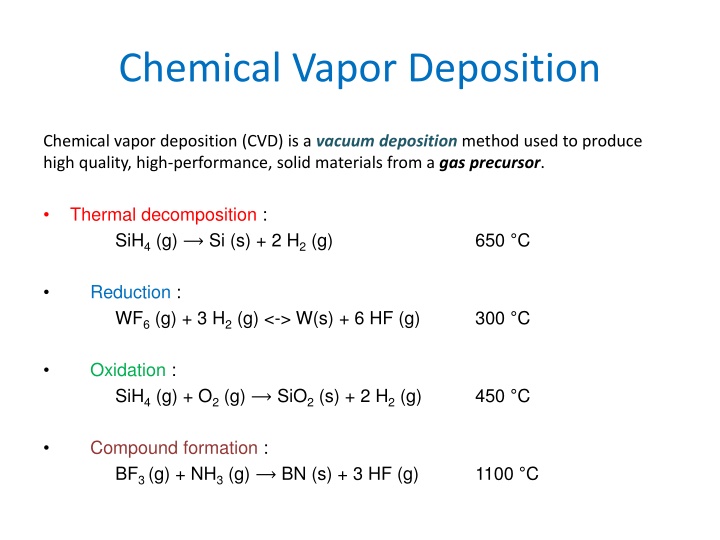
Chemical Vapor Deposition Chemical vapor deposition (CVD) is a vacuum deposition method used to produce high quality, high-performance, solid materials from a gas precursor. Thermal decomposition : SiH4(g) Si (s) + 2 H2(g) 650 C Reduction : WF6(g) + 3 H2(g) <-> W(s) + 6 HF (g) 300 C Oxidation : SiH4(g) + O2(g) SiO2(s) + 2 H2(g) 450 C Compound formation : BF3 (g) + NH3(g) BN (s) + 3 HF (g) 1100 C
Oxides preparation Various metal oxides can be prepared by the reaction of a volatile metal compound (often a chloride) with O2 or water vapor: MXn (g) + (n/4) O2 (g) MXn (g) + (n/2) H2O (g) MOn/2 (s) + n HX2 (g) MOn/2 (s) + (n/2) X2 (g) The water vapor can be directly introduced or obtain in the reaction chamber from a suitable reaction: 1) CO2 + H2 2) O2 + H2 H2O 3) CxHy + O2 CO2 + H2O CO + H2O 4
Chemical Vapor Deposition Ultrahigh vacuum CVD (UHVCVD) CVD at very low pressure, typically below 10 6 Pa ( 10 8 torr). Low-pressure CVD (LPCVD) CVD at sub-atmospheric pressures. Reduced pressures tend to reduce unwanted gas-phase reactions and improve product uniformity. Atmospheric pressure CVD (APCVD) CVD at atmospheric pressure.
LPCVD https://www.coursera.org/lecture/nanotechnology/chemical- vapor-deposition-process-demonstration-EWSQl
CVD Classification by type of substrate heating Hot wall CVD CVD in which the chamber is heated by an external power source and the substrate is heated by radiation from the heated chamber walls. Cold wall CVD CVD in which only the substrate is directly heated either by induction or by passing current through the substrate itself or a heater in contact with the substrate. The chamber walls are at room temperature.
CVD and Plasma methods Plasma is a state of matter in which an ionized gases becomes highly electrically conductive to the point that long-range electric and magnetic fields dominate the behavior of the matter. Plasma Enhanced CVD (PECVD) CVD that utilizes plasma to enhance chemical reaction rates of the precursors. PECVD processing allows deposition at lower temperatures, which is often critical in the manufacture of semiconductors. The lower temperatures also allow for the deposition of organic coatings, such as plasma polymers, that have been used for nanoparticle surface functionalization.
Direct synthesis of graphene on silicon oxide by low temperature plasma enhanced chemical vapor deposition Nanoscale, 2018,10, 12779-12787
Dissociation MW Plasma
https://www.youtube.com/watch?v=n4hjudErUsQ http://www.chm.bris.ac.uk/pt/diamond/mwpecvd1.htm
N-V center defect consists of a nitrogen atom in place of a carbon atom next to a vacancy within the diamond s lattice structure. Nitrogen-vacancy Center: the blue atoms represent Carbon atoms, red atom represents Nitrogen atom substituting for a Carbon atom, and yellow atom represents a lattice vacancy
Nanodiamonds: inertness and hardness Skin care: Nanodiamonds are well-absorbed by human skin. They also absorb more of the ingredients in skin care products than skin itself. Thus they cause more of the ingredients to penetrate the deeper layers of the skin. Nanodiamonds also form strong bonds with water, helping to hydrate the skin. Micro-abrasive: Polishes and engine oil additives for lubrication. Catalysis: Support or metal free catalyst Medical: low cytotoxicity of diamond nanoparticles affirms their utilization as biologically compatible materials. Drug delivery. Sensors: electro- mechanical- system and response to magnetic field. Optical and Quantum computing: Single-defect nanodiamonds.
Remote Plasma-Enhanced CVD (RPECVD) Similar to PECVD except that the wafer substrate is not directly in the plasma discharge region. Removing the wafer from the plasma region allows processing temperatures down to room temperature.
Low-Energy Plasma-Enhanced CVD (LEPECVD) CVD employing a high density, low energy plasma to obtain epitaxial deposition of semiconductor materials at high rates and low temperatures.
RF Plasma Synthesis https://www.youtube.com/watch?v=5Un_HnOl6lQ


")


")
")