Understanding Timing Diagrams and Machine Cycles in Microprocessors
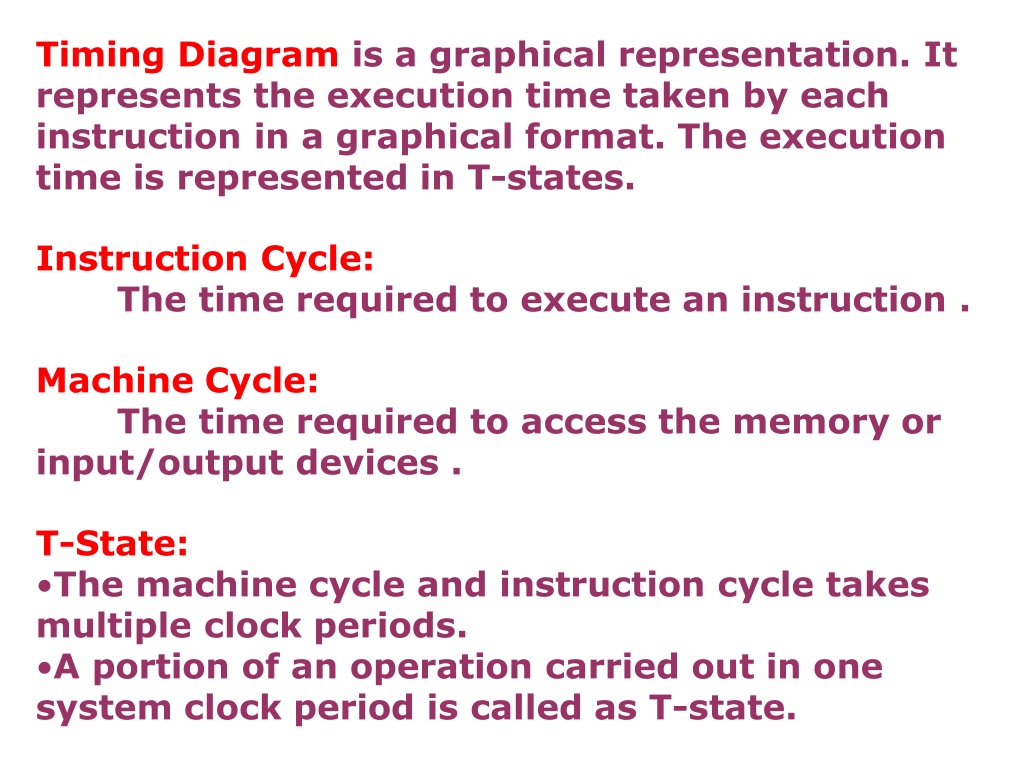
Timing
Diagram
is
a
graphical
representation.
It
represents
the
execution time taken
by
each
instruction in
a
graphical format. The execution
time
is
represented
in
T-states.
Instruction
Cycle:
The
time
required
to
execute
an
instruction
.
Machine
Cycle:
The
time required
to
access the memory
or
input/output
devices
.
T-State:
•
The machine cycle and
instruction
cycle takes
multiple
clock
periods.
•
A
portion
of
an
operation
carried out
in
one
system
clock
period is
called
as
T-state.
Timing
diagrams
•
The
8085
microprocessor
has 7 basic
machine
cycle.
They
are
1.
Op-code
Fetch
cycle(4T
or
6T).
2.
Memory
read
cycle
(3T)
3.
Memory write
cycle(3T)
4.
I/O
read
cycle(3T)
5.
I/O
write
cycle(3T)
6.
Interrupt
Acknowledge
cycle(6T
or 12T)
7.
Bus
idle
cycle
1.Opcode
fetch
cycle(4T
or
6T)
OPCODE
FETCH
•
The
Opcode
fetch
cycle,
fetches the
instructions from memory
and
delivers
it
to
the
instruction register of
the
microprocessor
•
Opcode
fetch
machine
cycle
consists
of
4
T-states
.
T1
State:
During the
T1
state, the
contents of
the
program counter
are
placed on the
16
bit
address
bus.
The
higher order
8
bits
are
transferred
to
address bus
(
A8-A15
) and
lower order
8
bits
are
transferred
to
multiplexed A/D
(
AD0-AD7
)
bus.
ALE (address latch
enable)
signal goes
high
.
As
soon
as
ALE goes
high,
the
memory
latches the
AD0-AD7 bus.
At
the
middle
of
the
T
state
the
ALE
goes
low
T2
State:
During the
beginning
of
this state, the
RD’
signal
goes
low
to enable memory. It
is
during this state, the selected
memory location is placed on D0-D7 of the Address/Data
multiplexed
bus.
T3
State:
In the previous state the Opcode is
placed
in D0-D7 of the A/D
bus.
In
this state
of
the
cycle, the
Opcode
of
the
A/D bus
is
transferred
to
the instruction register of
the
microprocessor.
Now
the
RD’
goes
high
after this
action
and
thus disables the
memory
from A/D bus.
T4
State:
In this
state
the
Opcode
which
was
fetched from the
memory
is
decoded.
2.
Memory
read
cycle
(3T)
•
These
machine cycles
have
3
T-states.
T1
state:
The
higher order address bus
(A8-A15)
and
lower order address
and
data multiplexed
(AD0-AD7)
bus.
ALE goes
high
so that
the
memory latches
the
(AD0-AD7) so that complete 16-bit address
are
available.
The
mp
identifies the
memory
read
machine
cycle
from
the
status signals
IO/M’=0, S1=1,
S0=0
.
This condition indicates the
memory
read
cycle.
T2
state:
Selected memory location is
placed on the
(D0-D7)
of
the
A/D
multiplexed
bus.
RD’ goes
LOW
T3
State:
The
data
which was loaded
on
the
previous state
is transferred
to
the
microprocessor.
In the
middle
of
the
T3
state
RD’
goes
high
and
disables the memory
read
operation. The
data
which
was
obtained from the
memory
is
then decoded.
•
•
•
3.
Memory
write
cycle
(3T)
•
•
These
machine cycles
have
3
T-states.
T1
state:
•
The
higher order address bus
(A8-A15)
and
lower order address
and
data multiplexed
(AD0-AD7)
bus.
ALE goes
high
so that
the
memory latches
the
(AD0-AD7) so that complete 16-bit address
are
available.
The
mp
identifies the
memory
read
machine
cycle
from
the
status signals
IO/M’=0, S1=0,
S0=1
.
This condition indicates the
memory
read
cycle.
T2
state:
Selected memory location is
placed on the
(D0-D7)
of
the
A/D
multiplexed
bus.
WR’ goes
LOW
T3
State:
•
In the middle of the
T3
state
WR’
goes
high
and
disables the
memory write operation
.
The
data which was obtained from
the memory is then decoded.
4.I/O
read
cycle(3T)
5.I/O
write
cycle(3T)
STA
instruction
ex:
STA
526A
It
require
4
m/c
cycles
13
T
states
1.opcode fetch(4T)
2.memory
read(3T)
3.memory
read(3T)
4.Memory
write(3T)
Timing
diagram
for
IN
C0
H
•
Fetching
the
Opcode
DB
H
from
the
memory
4125H.
•
Read
the
port
address
C0
H
from
4126
H
.
•
Read
the
content
of
port
C0
H
and
send
it
to
the
accumulator.
•
Let
the
content
of
port
is
5E
H
.
It
require
3
m/c
cycles
10
T
states
opcode
fetch(4T)
memory
read(3T)
I/O
read(3T)
OUT
instruction
Machines
Cycles(10T):
1.instruction
fetch(4T)
2.memory
read (3T)
3.IO
write
(3T)
Ti
m
in
g
diagra
m
f
o
r
MV
I
B
,
4
3
h
•
Fetching the
Opcode
06H
from the memory
2000
H
.
(OF
machine
cycle)
•
Read (move) the
data
43H
from memory
2001
H
.
(memory read)
I
N
R
M
A
D
D
M
references
•
8085
microprocessor
by
Sajid
Akram,
researcher/lecturer
at
c.abdul
hakeem college
of
engineering
and
technology
Timingdiagram
by
puja00
(slideshare.net)
Microprocessor
8086
by
Gopikrishna
Madanan,
Assistant
Professor
of
Physics
at
Collegiate
Education,
Kerala,
India
•
•

Timing diagrams provide a visual representation of execution times for instructions in a microprocessor, measured in T-states. This content delves into the concept of machine cycles, such as Opcode fetch cycle and Memory read cycle, in 8085 microprocessors. Exploring the T-states within each cycle, it explains the process of fetching, reading, and decoding instructions in detail.

Download Presentation

Please find below an Image/Link to download the presentation.
The content on the website is provided AS IS for your information and personal use only. It may not be sold, licensed, or shared on other websites without obtaining consent from the author. Download presentation by click this link. If you encounter any issues during the download, it is possible that the publisher has removed the file from their server.
E N D
Presentation Transcript
Timing Diagram is a graphical representation. It represents the execution time taken by each instruction in a graphical format. The execution time is represented in T-states. Instruction Cycle: The time required to execute an instruction . Machine Cycle: The time required to access the memory or input/output devices . T-State: The machine cycle and instruction cycle takes multiple clock periods. A portion of an operation carried out in one system clock period is called as T-state.
Timing diagrams The 8085 microprocessor has 7 basic machine cycle. They are 1. Op-code Fetch cycle(4T or 6T). 2. Memory read cycle (3T) 3. Memory write cycle(3T) 4. I/O read cycle(3T) 5. I/O write cycle(3T) 6. Interrupt Acknowledge cycle(6T or 12T) 7. Bus idle cycle
OPCODE FETCH The Opcode fetch cycle, fetches the instructions from memory and deliversit to the instruction register of the microprocessor Opcode fetch machine cycle consistsof 4 T-states. T1 State: During the T1 state, the contents of the program counter are placed on the 16 bit address bus. The higher order 8 bits are transferred to address bus (A8-A15) and lower order 8 bits are transferred to multiplexed A/D (AD0-AD7) bus. ALE (address latch enable) signal goes high. As soon as ALE goes high, the memory latches the AD0-AD7 bus. At the middle of the T state the ALE goes low
T2 State: During the beginningof this state, the RD signal goes low to enable memory. It is during this state, the selected memory location is placed on D0-D7 of the Address/Data multiplexed bus. T3 State: In the previous state the Opcode is placed in D0-D7 of the A/D bus. In this state of the cycle, the Opcode of the A/D bus is transferred to the instruction register of the microprocessor. Now the RD goes high after this actionand thus disables the memory from A/D bus. T4 State: In this state the Opcode which was fetched from the memory is decoded.
These machine cycles have 3 T-states. T1 state: The higher order address bus (A8-A15) and lower order address and data multiplexed (AD0-AD7) bus. ALE goes high so that the memory latches the (AD0-AD7) so that complete 16-bit address are available. The mp identifies the memory read machine cycle from the status signals IO/M =0, S1=1, S0=0. This condition indicates the memory read cycle. T2state: Selected memory location is placed on the (D0-D7) of the A/D multiplexed bus. RD goes LOW T3State: The data which was loaded on the previous state is transferred to the microprocessor.In the middle of the T3 state RD goes high and disables the memory read operation. The data which was obtained from the memory is then decoded.
These machine cycles have 3 T-states. T1 state: The higher order address bus (A8-A15) and lower order address and data multiplexed (AD0-AD7) bus. ALE goes high so that the memory latches the (AD0-AD7) so that complete 16-bit address are available. The mp identifies the memory read machine cycle from the status signals IO/M =0, S1=0, S0=1. This condition indicates the memory read cycle. T2state: Selected memory location is placed on the (D0-D7) of the A/D multiplexed bus. WR goes LOW T3State: In the middle of the T3 state WR goes high and disables the memory write operation. The data which was obtained from the memory is then decoded.
STA instruction ex: STA 526A
It require 4 m/c cycles 13 T states 1.opcode fetch(4T) 2.memory read(3T) 3.memory read(3T) 4.Memory write(3T)
Timing diagram for IN C0H Fetching the Opcode DBH from the memory 4125H. Read the port address C0H from 4126H. Read the content of port C0H and send it to the accumulator. Let the content of port is 5EH.
It require 3 m/c cycles 10 T states opcode fetch(4T) memory read(3T) I/O read(3T)
OUT instruction Machines Cycles(10T): 1.instruction fetch(4T) 2.memory read (3T) 3.IO write (3T)
Timing diagram for MVI B, 43h Fetching the Opcode 06H from the memory 2000H. (OF machine cycle) Read (move) the data 43H from memory 2001H. (memory read)
references 8085 microprocessor by Sajid Akram, researcher/lecturer at c.abdul hakeem college of engineering and technology Timingdiagram by puja00 (slideshare.net) Microprocessor 8086 by Gopikrishna Madanan, Assistant Professor of Physics at Collegiate Education, Kerala, India


")


")

")

")
")