Understanding the Organization of DRAM Subsystem Components
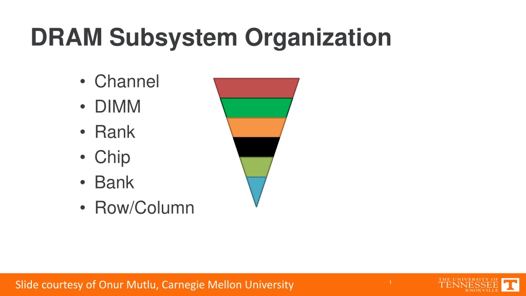
Explore the intricate structure of the DRAM subsystem, including memory channels, DIMMs, ranks, chips, banks, and rows/columns. Delve into the breakdown of DIMMs, ranks, chips, and banks to comprehend the design and functioning of DRAM memory systems. Gain insights into address decoding, row/column pairs, row buffer operations, and open/closed row policies in DRAM memory controllers. Courtesy of Onur Mutlu from Carnegie Mellon University.
- DRAM subsystem
- Memory channels
- DIMMs
- Ranks
- Chips
- Banks
- Rows
- Columns
- Address decoding
- Memory controllers

Download Presentation

Please find below an Image/Link to download the presentation.
The content on the website is provided AS IS for your information and personal use only. It may not be sold, licensed, or shared on other websites without obtaining consent from the author. Download presentation by click this link. If you encounter any issues during the download, it is possible that the publisher has removed the file from their server.
E N D
Presentation Transcript
DRAM Subsystem Organization Channel DIMM Rank Chip Bank Row/Column 1 Slide courtesy of Onur Mutlu, Carnegie Mellon University
The DRAM Subsystem Channel DIMM (Dual in-line memory module) Processor Memory channel Memory channel 2 Slide courtesy of Onur Mutlu, Carnegie Mellon University
Breaking Down a DIMM DIMM (Dual in-line memory module) Side view Front of DIMM Back of DIMM 3 Slide courtesy of Onur Mutlu, Carnegie Mellon University
Breaking Down a DIMM DIMM (Dual in-line memory module) Side view Front of DIMM Back of DIMM Rank 0: collection of 8 chips Rank 1 4 Slide courtesy of Onur Mutlu, Carnegie Mellon University
Rank Design Rank 0 (Front) Rank 1 (Back) <0:63> <0:63> Addr/Cmd CS <0:1> Data <0:63> Memory channel 5 Slide courtesy of Onur Mutlu, Carnegie Mellon University
Breaking Down a Rank . . . Chip 0 Chip 1 Chip 7 Rank 0 <56:63> <8:15> <0:7> <0:63> Data <0:63> 6 Slide courtesy of Onur Mutlu, Carnegie Mellon University
Breaking Down a Chip Chip 0 Bank 0 <0:7> <0:7> <0:7> ... <0:7> <0:7> 7 Slide courtesy of Onur Mutlu, Carnegie Mellon University
Breaking Down a Bank 2kB 1B (column) row 16k-1 ... Bank 0 row 0 <0:7> Row-buffer 1B 1B 1B ... <0:7> 8 Slide courtesy of Onur Mutlu, Carnegie Mellon University
Accessing DRAM Memory controller decodes each address into a <row,column> pair Open row policy: If the row buffer does not contain the proper row Precharge the row buffer to prepare to load the row Activate (RAS) opens row (places it into the row buffer) Read/write (CAS) reads/writes column in the row buffer Closed row policy: Activate (RAS) opens row (places it into the row buffer) Read/write (CAS) reads/writes column in the row buffer Precharge after every read/write (overlap with read/write) 9 Slide courtesy of Onur Mutlu, Carnegie Mellon University
Transferring a Cache Block Physical memory space 0xFFFF F Channel 0 ... DIMM 0 0x40 Rank 0 64B cache block 0x00 10 Slide courtesy of Onur Mutlu, Carnegie Mellon University
Transferring a Cache Block Physical memory space Chip 1 Chip 0 Chip 7 Rank 0 0xFFFF F . . . ... <56:63> <8:15> <0:7> 0x40 64B Data <0:63> cache block 0x00 11 Slide courtesy of Onur Mutlu, Carnegie Mellon University
Transferring a Cache Block Physical memory space Chip 1 Chip 0 Chip 7 Rank 0 0xFFFF F . . . Row 0 Col 0 ... <56:63> <8:15> <0:7> 0x40 64B Data <0:63> cache block 0x00 12 Slide courtesy of Onur Mutlu, Carnegie Mellon University
Transferring a cache block Physical memory space Chip 1 Chip 0 Chip 7 Rank 0 0xFFFF F . . . Row 0 Col 0 ... <56:63> <8:15> <0:7> 0x40 64B Data <0:63> cache block 8B 0x00 8B 13 Slide courtesy of Onur Mutlu, Carnegie Mellon University
Transferring a cache block Physical memory space Chip 1 Chip 0 Chip 7 Rank 0 0xFFFF F . . . Row 0 Col 1 ... <56:63> <8:15> <0:7> 0x40 64B Data <0:63> cache block 8B 0x00 14 Slide courtesy of Onur Mutlu, Carnegie Mellon University
Transferring a cache block Physical memory space Chip 1 Chip 0 Chip 7 Rank 0 0xFFFF F . . . Row 0 Col 1 ... <56:63> <8:15> <0:7> 0x40 64B Data <0:63> 8B cache block 8B 0x00 8B 15 Slide courtesy of Onur Mutlu, Carnegie Mellon University
Transferring a cache block Physical memory space Chip 1 Chip 0 Chip 7 Rank 0 0xFFFF F . . . Row 0 Col 1 ... <56:63> <8:15> <0:7> 0x40 64B Data <0:63> 8B cache block 8B 0x00 A 64B cache block takes 8 I/O cycles to transfer (4 total cycles with DDR). During the process, 8 columns are read sequentially. 16 Slide courtesy of Onur Mutlu, Carnegie Mellon University