Feedback Loop Compensation Design Using UCC28740 for Voltage Regulation
Explore the detailed design and control laws for a feedback loop compensation system using UCC28740 in a flyback regulator schematic diagram. The control law profile in CV mode, multiple control regions, and gain blocks are discussed for achieving high efficiency in voltage regulation. Gain blocks defined for output voltage sense and opto-coupler diode current provide insight into the control-loop gain factors. The voltage feedback loop block diagrams in FM and AM regions of the control law illustrate the control-loop gain equations for efficient operation.

Download Presentation

Please find below an Image/Link to download the presentation.
The content on the website is provided AS IS for your information and personal use only. It may not be sold, licensed, or shared on other websites without obtaining consent from the author. Download presentation by click this link. If you encounter any issues during the download, it is possible that the publisher has removed the file from their server.
E N D
Presentation Transcript
UCC28740 Feedback Loop Compensation Design 1
Flyback Regulator Schematic Diagram using UCC28740 with Opto-coupled Feedback + VF - VBULK VOUT NP NS + CB1 CB2 COUT VAC UCC28740 SOIC-7 RTL + VFA - VAUX VVDD VDD HV ROPT NA CVDD RS1 RFB1 VE VS DRV IOPT CFB3 RFB3 ZFB RS2 CS RLC FB TL431 RCS GND RFB2 IFB RFB4 2
UCC28740 Control Law for Output Voltage Regulation Control-Law Profile in Constant-Voltage (CV) Mode IPP(max) 100 kHz Multiple control regions modify switching frequency and inductor current amplitude to achieve high efficiency over wide output power range. IPP (peak primary current) IPP Control region 3 (AM) fSW fSW Control region 4 (FM) 32 kHz IPP(max) / 4 FM AM FM fSW(min) = 170Hz 3 kHz Control-loop gain factors change when operation moves from one region to another. 0 V 0.75 V 1.3 V 2.2 V 3.55 V 4.9 V 5 V Control region 1 (FM) Control Law Voltage, Internal - VCL Control region 2 (FM) 26 A 22.1 A 19.3 A 14.6 A 7.55 A 0.5 A Corresponding Feed-back Current, FB Input - IFB 3
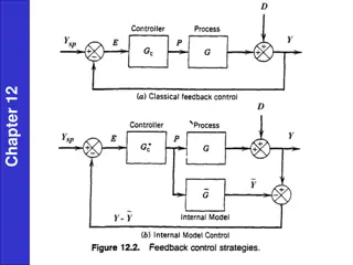
Voltage Feedback Loop Block Diagram in FM Regions of Control Law VIN IOUT + iO VOUT + vO GPn ZL(s) VCSn n = 1, 2, or 4, depending on FM region of operation fSW vO vCL iFB iE iD KFMn GFB2 GFB1 GOPTO(s) G431(s) Control-Loop Gain: AV = G431(s) GOPTO(S) GFB1 GFB2 KFMn GPn ZL(s) ??? ??? ??? ??? ???? ??? ???? ???? ???? ???? ??? ???? ??? ??? ??= 4
Voltage Feedback Loop Block Diagram in AM Region of Control Law VIN IOUT + iO VOUT + vO GP3 ZL(s) FAM vCS vO vCL iFB iE iD KAM GFB2 GFB1 GOPTO(s) G431(s) Control-Loop Gain: AV = G431(s) GOPTO(S) GFB1 GFB2 KAM3 GP3 ZL(s) ??? ??? ??? ??? ???? ??? ???? ???? ???? ???? ??? ???? ??? ??? ??= 5
Gain Blocks Defined G431(s) Output voltage sense to opto-coupler diode current gain: + VF - VBULK VOUT NP NS + CB1 CB2 COUT VAC UCC28740 SOIC-7 RTL + VFA - VAUX VVDD VDD HV ROPT NA CVDD RS1 iD 1 RFB1 VE ???= VS DRV ??? IOPT CFB3 RFB3 ZFB RS2 CS RLC FB TL431 RCS GND RFB2 IFB RFB4 ??? ??? 1 1 + ??????1 ??????1 ?431? = ??? 6
Gain Blocks Defined GOPTO(s) Opto-coupler diode current to emitter current gain: + VF - UCC28740 VBULK VOUT VVDD NP NS + VDD CB1 CB2 COUT COPTO VAC CCE UCC28740 SOIC-7 RTL + VFA - VAUX VVDD CFB3 RFB3 VDD HV ROPT NA CVDD VFB FB RS1 iD RFB1 iE VE VS DRV IOPT REQU CFB3 RFB3 RFB4 ZFB RS2 CS RLC VEQU FB TL431 RCS GND RFB2 IFB RFB4 GND ??= ?????+ ??? ??? ??? 1 ?????? = ??? ???3 ?? 1 + ??????4 ???? 7 CCE is external capacitance added across opto-coupler, if necessary
Gain Blocks Defined GFB1 Opto-coupler emitter current to FB-pin current gain: UCC28740 + VF - VBULK VOUT VVDD NP NS VDD + CB1 CB2 COUT COPTO VAC CCE UCC28740 SOIC-7 RTL iE + VFA - CFB3 RFB3 VAUX VVDD VDD HV ROPT NA iFB CVDD VFB FB RS1 RFB1 VE VS DRV REQU IOPT CFB3 RFB3 RFB4 ZFB RS2 CS RLC VEQU FB TL431 RCS GND RFB2 IFB RFB4 GND ???? ??? ???4 ???1= = ???4+ ???? 8
Gain Blocks Defined GFB2 FB-pin current to Control-Law voltage gain: UCC28740 UCC28740 VVDD VVDD VDD VDD COPTO COPTO CCE CCE 5 V CFB3 CFB3 RFB3 RFB3 480 k iFB iFB VFB VFB FB FB VCL IFB REQU REQU RFB4 RFB4 IFB / 2.5 VEQU VEQU GND GND ???? ???? 480? 2.5 ???2= = 9
Gain Blocks Defined KFMn, KAM3 Control-Law voltage to power stage modulation (FM or AM) gain: UCC28740 VVDD Control-Law Profile in Constant-Voltage (CV) Mode VDD IPP(max) ???4= 50.4??? ? 100 kHz COPTO IPP (peak primary current) CCE IPP fSW 5 V fSW ???3= 0.433? ? CFB3 RFB3 480 k 32 kHz VFB FB IPP(max) / 4 FM AM FM VCL ???2= 32.2??? ? fSW(min) = 170Hz IFB 3 kHz REQU RFB4 IFB / 2.5 0 V 0.75 V 1.3 V 2.2 V 3.55 V 4.9 V 5 V Control Law Voltage, Internal - VCL VEQU ???1= 5.1??? ? 26 A 22.1 A 19.3 A 14.6 A 7.55 A 0.5 A GND Corresponding Feed-back Current, FB Input - IFB ???? ???? 50.4??? ? ???? ???? 0.433? ? ???4= = ???3= = 10
Gain Blocks Defined GPn, GP3 Power stage modulation (FM or AM) to average current gain: + VF - VBULK VOUT NP NS + CB1 CB2 COUT VAC UCC28740 SOIC-7 RTL + VFA - VAUX VVDD VDD HV ROPT NA CVDD RS1 RFB1 VE VS DRV IOPT CFB3 RFB3 ZFB RS2 CS RLC FB TL431 RCS GND RFB2 IFB RFB4 2 ??? ???? ???? ???? ??? ????? 1 ??? ???? ???? ???? ?? 2 ???= = ??3= = ??? ???? ????? ?????? IPn = IPMAX for n = 4; = IPMAX/4 for n = 1, 2 IP = Primary peak current at specific load condition FAM = AM region switching frequency 11
Gain Blocks Defined ZL(s) Output current to output voltage gain: + VF - VBULK VOUT RL NP NS + CB1 CB2 COUT VAC Output impedance, ZL(s), comprises output capacitance in parallel with load resistance. UCC28740 SOIC-7 RTL + VFA - VAUX VVDD VDD HV ROPT NA CVDD RS1 RFB1 VE VS DRV IOPT CFB3 RFB3 ZFB RS2 CS RLC FB Factor of is due to differentiation. TL431 RCS GND RFB2 IFB RFB4 RL = VOUT/IOUT at specific condition of interest. ??? ??? ?? 2 1 ??? = = 1 + ??????? 2 12
Full Loop-gain Equation Control-Loop Gain: AV = G431(s) GOPTO(S) GFB1 GFB2 KFMn GPn ZL(s) ??? ??? ??? ??? ???? ??? ???? ???? ???? ???? ??? ???? ??? ??? ??= ?? 1 1 + ??????1 ??????1 50.4??? 1 ???4 ??? ??? 480? 2.5 ???4+ ???? 1 1 + ??????? 1 + ??????4 ???? ????? ????? 2 ???? ???? 1 ?? 2 ? ???? 2 13
Design Considerations ?? 1 1 + ??????1 ??????1 50.4??? 1 ???4 ??? ??? 480? 2.5 ???4+ ???? 1 1 + ??????? 1 + ??????4 ???? ????? ????? 2 ???? ???? 1 ?? 2 ? ???? 2 Limited flexibility of choice for several component values: REQU = device parameter, inflexible value PMAX, FMAX, and COUT are determined during DC design RTL and RFB4 have narrow variability after nominal DC design consideration CTR has limited choice of rankings CP can only be made larger (using external CCE), not smaller RFB1 and CZ have wider range of values to set compensation zero 14
Design Considerations Generate Bode-plot gain and phase of AV at full-load condition with CZ = 0. ?? 1 1 1 1 ???4 ??? ??? 480? 2.5 ???4+ ???? 1 ???? 1 + ??????4 ???? 50.4??? ? ???? 2 ???? ????? ????? ?? 2 1 1 + ??????? 2 From plot, determine the frequency (fZ) where placing a zero in the response would cause the response to cross 0dB with at least 45 phase margin. Calculate CZ = 1/(2 fZRFB1) If necessary, adjust CP with CCE such that the loop cross-over frequency < 3 kHz. Iterate and fine-tune loop compensation during prototype evaluation. 15
Simplifying Assumptions TL431, CTR: The gain of these components do have high-frequency roll-off characteristics (pole) but are considered constant provided the loop crossover frequency is significantly lower than their respective pole frequencies. REQU is linearized from a piece-wise linear approximation of the VFB/IFB curve. The ESR-zero frequency of COUT is far above the loop crossover frequency. CFB3 is more than 10 times larger than CP which causes its effect on compensation to be negligible. The product gMRTL > 10000, which causes several terms to become negligible (gM = transconductance of TL431). 16


")
")


")