Understanding Nanoscale Lithography Techniques

Nanoscale lithography is a crucial fabrication process driven by technology demands for smaller and faster devices. This article explores lithography techniques like photolithography, electron beam lithography, and x-ray lithography, essential for fabricating nanostructures and enhancing performance in modern technology. Discover the process, key terms, and insights into nanoscale lithography in this detailed overview.
- Nanoscale Lithography
- Fabrication Techniques
- Photolithography
- Electron Beam Lithography
- X-Ray Lithography

Download Presentation

Please find below an Image/Link to download the presentation.
The content on the website is provided AS IS for your information and personal use only. It may not be sold, licensed, or shared on other websites without obtaining consent from the author. Download presentation by click this link. If you encounter any issues during the download, it is possible that the publisher has removed the file from their server.
E N D
Presentation Transcript
NANOSCALE LITHOGRAPHY MICHAEL JOHNSTON 4/13/2015
ABSTRACT AND OUTLINE Overview(What, Why, Nano) Photolithography Electron Beam Lithography X-Ray Lithography Conclusion References Concept Check Nanoscale Lithography is an ever growing fabrication process due to technology demands. We are continuously striving to increase the number of transistors on a chip to increase performance. The drive for smaller and faster technologies has caused the development of fabrication techniques that allow us to work at the nanoscale feature size. A few lithography techniques will be explored to show how this whole process works. The processes I will cover include Photo, Electron Beam and X-Ray lithography. These forms of lithography share a common process of preparation exposure and development while fabricating wafers. Key Terms: Photolithography, Electron Beam Lithography, X-Ray Lithography, Photo Resist, Electron Scattering, Photo Mask, Ionization
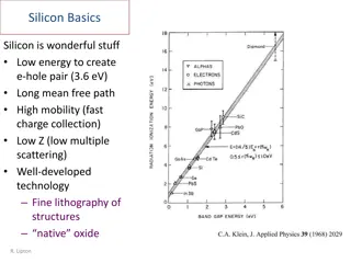
WHAT IS LITHOGRAPHY!? The process of transferring or printing a pattern from one medium to another Johann Alois Senefelder (1796), used ink on limestone
TECHNOLOGY TRENDS Moore s Law Smaller, Faster, Cheaper Performance
NANOSCALE LITHOGRAPHY Using Lithographic tools for fabrication of any structures having feature size of less than 100 nm Human hair is ~80,000 nm thick Downscale feature size, high throughput and quality
FORMS OF LITHOGRAPHY Photo Electron Beam X-Ray Projection Printing Direct Writing Proximity Printing
PHOTOLITHOGRAPHY UV light passes through focusing lenses and masks to react with a photoresist to form patterns on a wafer Projection Printing Technique Limited by diffraction limit
PHOTOLITHOGRAPHY PROCESS General Steps: 1. Substrate preparation 2. Photoresist 3. Alignment and Masking 4. Development
PHOTOLITHOGRAPHY PROCESS 1. SUBSTRATE PREPARATION Use modern clean rooms with robotic wafer cleaning systems Surface Impurities are removed by wet chemical treatment Baked to remove moisture 2. PHOTORESIST Apply a layer of resist that will react to the light Evenly coated by spin coating
PHOTOLITHOGRAPHY PROCESS ALIGNMENT AND MASKING Wafer is carefully aligned using automated mechanical process Mask is aligned over wafer with desired pattern DEVELOPMENT Developed using liquid solvent Wet or Dry Etching performed on substrate Photo Resist strip
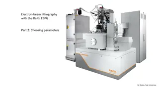
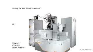
ELECTRON BEAM LITHOGRAPHY (EBL) Highly focused electron beam is exposed to a resist material that modifies the solubility of the resist for development Allows accuracy down to as small as 10nm dimensions Nanoscale design is done on computers and the pattern is written on a chip using highly precise mechanical devices Goals of EBL writing are highly accurate and reliable pattern writing
LIMITING FACTORS IN EBL Quality of the Electron Optics Choice of Substrate, Resist, Developer Electron Beam Energy Level and Dose Development Time and Temperature Electron Scattering
ELECTRON SCATTERING Mutual repulsive forces from the electrons charges-worse at higher currents and lower energy levels Gas Scattering-reduced by using a vacuum Forward and Back Scattering Ionization (Secondary Electron Generation)
ELECTRON SCATTERING Forward Scattering- electrons entering resist undergo low energy inelastic collisions which deflect the electrons slightly causing the beam to widen Back Scattering-electrons pass through the resist into substrate and undergo enough collisions to deflect and reemerge into the resist causing proximity issues
EBL RESISTS Positive Resist: Converts from low to high solubility when exposed to electrons PMMA (poly-methyl methacrylate)- longer polymer chain which is broken up into smaller more soluble chains Negative Resist: Converts to low solubility when exposed to electron beam HSQ (hydrogen silsesquioxane)- undergoes polymer cross-linking to form longer less soluble chains
DEVELOPMENT After exposure, resist is immersed in a liquid solvent to dissolve the fragments (positive) or non cross-linked molecules (negative). Temperature and duration are a large factor here Cold treat PMMA for higher resolution
ELECTRON ENERGY LEVEL Inelastic cross sectional area decreases proportionately to electron energy increasing In positive resists this causes fewer chain scissions per electron resulting in a lower sensitivity Electrons with higher energy levels undergo less forward scattering, resulting in a narrower electron beam Higher energy electrons penetrate deeper into the substrate causing proximity issues
X-RAY LITHOGRAPHY Parallel Proximity Printing X-Ray lithography uses ultra thin masks ( <2 micro) X-Rays pass directly through mask and onto wafer Shorter wavelength than UV (0.4- 4nm)
CHALLENGES OF X-RAY LITHOGRAPHY The thin masks are prone to deform due to small stresses Masks deformation is huge in XRL because of the direct mapping X-Rays cannot be focused through a lens
CONCLUSION PHOTO X-RAY ELECTRON BEAM UV Light Proximity Printing Direct Writing Limited by UV Wavelength Efficient Expensive Projection Printing Accurate Highly Accurate Expensive/Fragile Masks Low Throughput Primarily Used to develop masks for X- Ray
REFERENCES Stepanova, Maria, and Steven Dew. Nanofabrication: Techniques and Principles. Wien: SpringerWienNewYork, 2012. Print. Jackson, M. J. "Microfabrication Using X-Ray Lithography" Micro and Nanomanufacturing Springer, 2007. Print. H. J. Levinson, Principles of Lithography, Second Edition, SPIE Press, Bellingham, WA (2005). Available at: http://spie.org/x33182.xml Pictures: Senefelder http://en.wikipedia.org/wiki/Alois_Senefelder#/media/File:Senefelder.jpg Moore s Law http://www.cuug.ab.ca/~branderr/eeepc/016_moores_law_intel.html Hair http://waynesword.palomar.edu/lmexer1.htm E-Beam Lithography http://www.ece.umd.edu/class/enee416/GroupActivities/Ebeam.pdf
CONCEPT CHECK Describe the basic lithographic process What types of resist are used, and what are the differences between them? What are the three lithographic processes and what type of printing do they perform? What is forward and back scattering and how do they effect the fabrication process? What is a drawback of EBL?


")