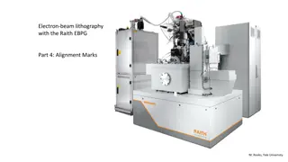
Electron Beam Lithography with Raith EBPG: Alignment Marks Guide
The use of alignment marks in electron-beam lithography is crucial for aligning different layers of lithography, enabling precise printing of intricate patterns like wires connecting pads. This guide explores the significance of alignment marks, common alignment strategies, differences in alignment
0 views • 13 slides
Exploring Nanotechnology at Photonics Center - An Introduction to the Nanoscale
Delve into the fascinating world of nanotechnology with Professor Helen Fawcett at the NSF REU and RET at Photonics Center. Discover the significance of a nanometer, compare nanoscale sizes to visible objects, and learn about the wonders of nanotechnology in interdisciplinary science and engineering
0 views • 9 slides
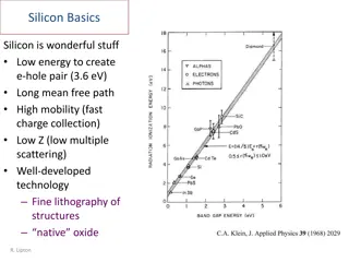
Understanding Silicon Detector Technology
Silicon is a remarkable material with low energy requirements for creating e-hole pairs, long mean free paths, high mobility for fast charge collection, and well-developed technology for fine lithography. Silicon detectors operate based on carrier band diagrams, density of states, and Fermi-Dirac di
0 views • 21 slides
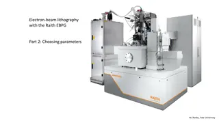
Choosing Parameters for Electron-Beam Lithography with the Raith EBPG
In the process of electron-beam lithography with the Raith EBPG, selecting parameters such as resist type, resist thickness, spot size, dose range, resist sensitivity, and beam step size is crucial for achieving precise patterns. Factors like the substrate, developer, and pattern transfer technique
0 views • 9 slides
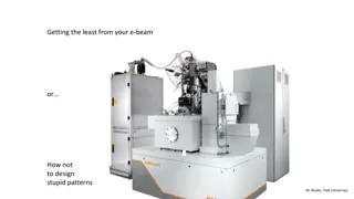
Optimizing E-Beam Design: Settling Time and Avoiding Costly Mistakes
Dive into the intricacies of E-beam lithography design, focusing on the crucial aspects of settling time, polygonal shapes over circles, and the impact of dot size on pattern generation efficiency. Learn how to minimize settling time, reduce costs, and maximize output quality in your E-beam designs.
0 views • 19 slides

Understanding Proximity Effect in Electron Beam Lithography
Explore the impact of proximity effect in EBL, its causes, and its effects on resolution. Learn about physical models, reduction techniques, and correction methods to mitigate proximity effect and enhance lithographic precision.
0 views • 11 slides

Advancements in Nanomaterials for Building Construction
Addition of nanoscale materials like nano-SiO into cement can enhance compressive strength and pore size distribution in concrete. Carbon nanotubes offer mechanical durability and crack prevention in construction materials. However, the use of nanomaterials in construction is currently limited due t
0 views • 22 slides
Advanced Microscopy Techniques in EUV Lithography: SHARP Overview
SHARP utilizes Fresnel zone plate lenses to achieve diffraction-limited quality in EUV lithography, offering a range of NA values and image magnifications. The system allows emulation of mask-side imaging conditions with hundreds of lenses available. Coherence control and engineering are provided th
0 views • 18 slides
Next-Generation Photomasks in Extreme Ultraviolet Lithography Symposium
Explore the latest advancements in actinic mask imaging and semiconductor high-NA reticle technology presented at the 2015 International Symposium on Extreme Ultraviolet Lithography in Maastricht. Topics include zoneplate lenses, phase reconstruction algorithms, Fourier Ptychography microscopy, and
0 views • 56 slides
Industrialization Process for Mass Production: Plan A vs. Plan B
Various industrialization plans for mass production are compared, focusing on the advantages and challenges of Prototype production in an institute followed by mass production in an industrial company (Plan A) versus having the prototype made by an industrial company from the beginning (Plan B). Cas
0 views • 9 slides
Utah Valley University - Virtual Reality Implementation for Nanotechnology Education
Utah Valley University (UVU) introduces a nanotechnology course this fall, leveraging VR simulations to train students in nanofabrication and characterization techniques such as photolithography, electron beam lithography (EBL), sputtering, and microscopy. The VR simulations help students familiariz
0 views • 8 slides
Comparative Analysis of Bottom-up and Top-down Nanomaterial Synthesis Techniques
Bottom-up techniques yield individual nanoparticles with narrow size distributions, while top-down methods produce bulk nanostructured materials. Physical Vapour Deposition (PVD) and Inert Gas Condensation (IGC) are examples of bottom-up approaches capable of synthesizing nanomaterials with precise
0 views • 10 slides
Laser Ablation for Generation of Nanoparticles and Nanowires: Workshop Insights
Explore the latest research on laser ablation techniques for generating nanoparticles and nanowires, presented at the Si-W Ecal Workshop in Korea. Discover the various methods, applications in solar cells and LEDs, and the use of semiconductor materials. Learn about the advanced 20-TW laser system a
0 views • 31 slides

Understanding Double Patterning Lithography Techniques
Explore the world of lithography with a focus on double patterning techniques. From self-aligned double patterning to chemical vapor deposition methods, this comprehensive overview covers the key concepts, challenges, and solutions in advanced semiconductor manufacturing processes. Dive into the int
0 views • 28 slides
Advances in Ceramic Composite Property Modeling and Experimental Characterization
European research focuses on advanced modeling of C/C, C/SiC, and SiC/SiC composites for aerospace and nuclear applications, with an emphasis on correlating simulations with experimental validation. Laboratories are progressing towards a multiscale approach, integrating micro/nanomechanical characte
0 views • 5 slides
Exploring Nanoscience and Nanotechnology with Dr. Abeer Alshammari
Delve into the fascinating world of nanoscience and nanotechnology through the elective course PHYS 476 with Dr. Abeer Alshammari. Learn about the unique properties of nanomaterials, including microstructure, defects, dislocations, twins, stacking faults, and more. Discover how nano-dimensions impac
0 views • 10 slides
Exploring Atomic Dimensions: Scanning Probe Microscopy
Delve into the world of nanoscale imaging with Scanning Probe Microscopy (SPM) techniques like Scanning Tunneling Microscopy (STM) and Atomic Force Microscope (AFM). Unlike optical microscopes, SPM methods break the diffraction limit by relying on intermolecular forces and quantum tunneling for unpa
0 views • 26 slides
Understanding Classification of Nanomaterials and Quantum Phenomena
Nanomaterials are classified into different types such as nanocrystals and quantum dots, each exhibiting unique properties at the nanoscale. Quantum dots, zero-dimensional systems, show quantum confinement effects leading to tuneable light emission. One-dimensional structures like nanowires and nano
0 views • 18 slides
Understanding Nanoscale Lithography Techniques
Nanoscale lithography is a crucial fabrication process driven by technology demands for smaller and faster devices. This article explores lithography techniques like photolithography, electron beam lithography, and x-ray lithography, essential for fabricating nanostructures and enhancing performance
0 views • 24 slides