Understanding Diodes: Construction, Characteristics, and Applications
Explore the world of diodes through detailed explanations of construction methods, electrical characteristics, and V-I characteristic curves. Learn about forward and reverse biasing, diode applications, and diodes used as rectifiers. Delve into alloyed and diffused junctions, PN junction basics, barrier voltage, and diode packaging. Understand forward bias behavior and voltage drops in diodes.
Download Presentation

Please find below an Image/Link to download the presentation.
The content on the website is provided AS IS for your information and personal use only. It may not be sold, licensed, or shared on other websites without obtaining consent from the author. Download presentation by click this link. If you encounter any issues during the download, it is possible that the publisher has removed the file from their server.
E N D
Presentation Transcript
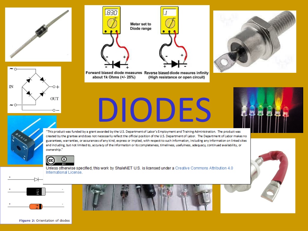
ENABLING OBJECTIVES 1.1 Describe the construction methods for manufacturing PN junction diodes 1.2 Explain in detail the electrical characteristics of the PN junction diode 1.3 Explain the Voltage-Current (V-I) characteristic curve for semiconductor diodes. 1.4 Explain forward and reverse semiconductor diode biasing. 1.5 Identify the parts of a diode on both an actual device and the schematic symbol of a diode. 1.6 List the basic application where diodes are utilized. 1.7 Explain the operation of a diode when used as a rectifier. 3
ALLOYED PN JUNCTION The materials are heated until the indium pellet melts and partially fuses with the N-type material, forming a PN junction. 4
DIFFUSED JUNCTION The most widely used method of making semiconductor diodes is by diffusion. The operation occurs at a very high temperature and the gaseous doping atoms penetrate, or diffuse, into the exposed surfaces of the N-type material, resulting in a PN junction. 5
PN JUNCTION N-type material is the Cathode P-type material is the Anode Both the P-type and the N-type material are electrically neutral. 6
BARRIER VOLTAGE The combination of the majority carriers at the junction results in a barrier voltage. 7
FORWARD BIAS Anode Cathode Majority carriers are forced toward the junction where they will combine. 10
FORWARD BIAS Anode Cathode Current Flow - + The forward voltage drop (Vf) is typically 0.7V for a silicon diode and 0.3V for a germanium diode. 11
FORWARD BIAS ED1 = 0.7V - + - ER1 = E - 0.7V + I = ER1 / R1 12
FORWARD BIAS If E = 15V, D1 is silicon, and R1 = 1K , what is the circuit current and the voltage across D1 and R1? 13
REVERSE BIAS Majority carriers are drawn away from the junction enlarging the depletion region. 14
REVERSE BIAS - + The maximum reverse bias voltage that the diode can withstand is it s peak inverse voltage rating (PIV). 15
REVERSE BIAS ED1 = E - + ER1 = 0V I = 0A A theoretically perfect diode has no leakage current. In reality, a small leakage current flows. Germanium diodes exhibit a greater leakage current than silicon diodes. 16
FORWARD/REVERSE BIAS Reverse bias current is due to leakage. 17
GERMANIUM vs. SILICON Germanium Silicon Low forward voltage drop Reverse leakage current Higher forward voltage drop Minimal reverse leakage current 21
CONVENTIONAL FULL WAVE RECTIFIER 23
FULL WAVE BRIDGE RECTIFIER 24
ENABLING OBJECTIVES 1.1 Describe the construction methods for manufacturing PN junction diodes 1.2 Explain in detail the electrical characteristics of the PN junction diode 1.3 Explain the Voltage-Current (V-I) characteristic curve for semiconductor diodes. 1.4 Explain forward and reverse semiconductor diode biasing. 1.5 Identify the parts of a diode on both an actual device and the schematic symbol of a diode. 1.6 List the basic application where diodes are utilized. 1.7 Explain the operation of a diode when used as a rectifier. 26
