TUNNEL DIODE
Tunnel diodes, with their unique negative resistance characteristic, have revolutionized electronics since their invention by Leo Esaki in 1957. Explore the working principle, applications like tunnel diode oscillators, and the intriguing tunneling effect in this fascinating semiconductor device.

Download Presentation

Please find below an Image/Link to download the presentation.
The content on the website is provided AS IS for your information and personal use only. It may not be sold, licensed, or shared on other websites without obtaining consent from the author.If you encounter any issues during the download, it is possible that the publisher has removed the file from their server.
You are allowed to download the files provided on this website for personal or commercial use, subject to the condition that they are used lawfully. All files are the property of their respective owners.
The content on the website is provided AS IS for your information and personal use only. It may not be sold, licensed, or shared on other websites without obtaining consent from the author.
E N D
Presentation Transcript
TUNNEL DIODE Dr.A.ANBARASI ASSOCIATE PROFESSOR DEPARTMENT OF PHYSICS PERIYAR ARTS COLLEGE CUDDALORE
TUNNEL DIODE SYMBOL It was invented by Leo Esaki in August1957 The cathode and anode are the two terminals of the semiconductor material. The diode has effectively Negative resistance due to quantum mechanical effect
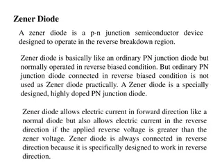
Definition of tunnel diode A tunnel diode is a heavily doped p-n junction diode in which the electric current decreases as the voltage increases. In tunnel diode electric current is caused by tunneling. The tunnel diodes are very fast switching devices. Eg:computers switches, very high frequency oscillators and amplifiers
APPLICATION; TUNNEL DIODE OSCILLATOR The resistance is the parallel equivalent of the winding resistance of the coil. When a tank circuit is set into oscillations by applying voltage, damped oscillations are produced. This is because of energy lost in the resistance of the tank circuit. UNDAMPED OSCILLATIONS; The negative resistance oscillator is constructed using tunnel diode. The negative resistance characteristic of the tunnel diode counteracts the positive resistance of the tank circuit, so undamped oscillation is produced at the output.
Tunneling effect In electronics, Tunneling is known as a direct flow of electrons across the small depletion region from n-side conduction band into the p-side valence band. In a p-n junction diode, both positive and negative ions form the depletion region. Due to these ions, in-built electric potential or electric field is present in the depletion region. This electric field gives an electric force to the opposite direction of externally applied voltage.
Tunnel diode (V-I) characteristics when forward voltage increases from zero, the forward current quickly reaches the peak value Ip when a particular low forward voltage Vp is the lower forward voltage It exceeds Vp the forward current decreases and reaches minimum value Called valley current Ip at valley voltage Vv. The region between the peak current Ip and the valley current Iv is called Negative resistance region. Forward voltage is further increased beyond the valley point the current increases again as an ordinary p-n junction diode
Forward current in a tunnel diode. It is the sum of two components due to two different mechanisms 1)NORMAL INJECTION CURRENT: It arises from an external voltage which reduces the potential barrier across the depletion region and allows current to flow due to majority carriers in the conduction band. It is shown by dashed curve. 2)TUNNEL CURRENT: In a tunnel diode due to heavy doping,the depletion region is very narrow. It results in a very high electric field across the junction and allows carriers in the valence energy band on one side of the junction to tunnel through to the conduction energy band on the other side of the junction without overcoming the potential barrier. The increase in current from 0 to its peak value Ip at a forward voltage Vp is due to tunneling phenomenon.
Tunnel diode applications; Applications of Tunnel Diode Tunnel diode can be used as a switch, amplifier, and oscillator. Since it shows a fast response, it is used as high frequency component. Tunnel diode acts as logic memory storage device. They are used in oscillator circuits, and in FM receivers. Since it is a low current device, it is not used more.
HALF WAVE RECTIFIER Dr.A.ANBARASI ASSOCIATE PROFESSOR DEPARTMENT OF PHYSICS PERIYAR ARTS COLLEGE CUDDALORE
Half wave rectifier Ahalf wave rectifier is defined as a type of rectifier that only allows one half- cycle of an AC voltage waveform to pass, blocking the other half-cycle. Half- wave rectifiers are used to convert AC voltage to DC voltage, and only require a single diode to construct.
WORKING OF HALF WAVE RECTIFIER In the positive half cycles when the input AC power is given to the primary winding of the step down transformer, we will get the decreased voltage at the secondary winding which is given to the diode. The diode will allow current flowing in clock wise direction from anode to cathode in the forward bias (diode conduction will take place in forward bias) which will generate only the positive half cycle of the AC. The diode will eliminate the variations in the supply and give the pulsating DC voltage to the load resistance RL. We can get the pulsating DC at the Load In the negative half cycle the current will flow in the anti-clockwise direction and the diode will go in to the reverse bias. In the reverse bias the diode will not conduct so, no current in flown from anode to cathode, and we cannot get any power at the load resistance. Only small amount of reverse current is flown from the diode but this current is almost negligible. And voltage across the load resistance is also zero.
The main supply voltage is given to the transformer which will increase or decrease the voltage and give to the diode. In most of the cases we will decrease the supply voltage by using the step down transformer here also the output of the step down transformer will be in AC. This decreased AC voltage is given to the diode which is connected serial to the secondary winding of the transformer, diode is electronic component which will allow only the forward bias current and will not allow the reverse bias current. From the diode we will get the pulsating DC and give to the load resistance RL
RIPPLE FACTOR OF HALF WAVE RECTIFIER Ripple is the unwanted AC component remaining when converting the AC voltage waveform into a DC waveform. Even though we try out best to remove all AC components, there is still some small amount left on the output side which pulsates the DC waveform. This undesirable AC component is called ripple . To quantify how well the half-wave rectifier can convert the AC voltage into DC voltage, we use what is known as the ripple factor (represented by or r). The ripple factor is the ratio between the RMS value of the AC voltage (on the input side) and the DC voltage (on the output side) of the rectifier.
A half wave rectifier is rarely used in practice. It is never preferred as the power supply of an audio circuit because of the very high ripple factor. High ripple factor will result in noises in the input audio signal, which in turn will affect audio quality. The advantage of a half wave rectifier is only that its cheap, simple and easy to construct. It is cheap because of the low number of components involved. Simple because of the straight forwardness in circuit design. Apart from this, a half wave rectifier has more number of disadvantages than advantages!


 characteristics")
 characteristics")