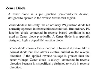
Diode Junction Biasing: Zero and Forward Bias Conditions

In the world of electronics, diode junction biasing plays a crucial role. This article delves into the concepts of zero and forward bias conditions for diodes. When a diode is zero-biased, no external potential energy is applied, while in forward bias, a specific voltage is introduced to initiate current flow. Understanding these bias conditions is essential for comprehending diode behavior and circuit operation.

Download Presentation

Please find below an Image/Link to download the presentation.
The content on the website is provided AS IS for your information and personal use only. It may not be sold, licensed, or shared on other websites without obtaining consent from the author.If you encounter any issues during the download, it is possible that the publisher has removed the file from their server.
You are allowed to download the files provided on this website for personal or commercial use, subject to the condition that they are used lawfully. All files are the property of their respective owners.
The content on the website is provided AS IS for your information and personal use only. It may not be sold, licensed, or shared on other websites without obtaining consent from the author.
E N D
Presentation Transcript
ZERO BIASED JUNCTION DIODE ZERO BIASED JUNCTION DIODE When a diode is connected in a Zero condition, no external potential energy is applied to the PN junction. However, if the diodes terminals are shorted together, a few holes (majority carriers) in the P-type material with enough energy to overcome the potential barrier will move across the junction against this barrier potential. This is known as the Forward and is referenced as I IF F. Likewise, holes generated in the N-type material (minority carriers), move across the junction in the opposite direction. This is known as the Reverse Reverse Current Current and is referenced as I IR R. This transfer of electrons and holes back and forth across the P-N junction is known as diffusion Zero Bias Bias Forward Current Current diffusion.
The discourages the diffusion of any more majority carriers across the junction. However, the potential barrier helps minority carriers (few free electrons in the P-region and few holes in the N-region) to drift across the junction. Then an Equilibrium Equilibrium or balance balance will be established when the majority carriers are equal and both moving in opposite directions, so that the net result is zero zero current current flowing in the circuit. When this occurs the junction is said to be in a state of Dynamic Dynamic Equilibrium Equilibrium. potential barrier that now exists
FORWARD BIAS JUNCTION DIODE FORWARD BIAS JUNCTION DIODE When a diode is connected in a Forward Bias condition, a negative voltage is applied to the N-type material and a positive voltage is applied to the P-type material (the p side connected to the more positive potential than the n side.). Forward Bias
If this external voltage becomes greater than the value of the potential barrier (approx. volts for silicon and volts for silicon and 0.3 0.3 volts for germanium) the potential barriers will be overcome and current will start to flow. (approx. 0.7 0.7 volts for germanium)
This This is is because electrons towards the junction giving them the energy to cross over and combine with the holes being pushed in the opposite direction towards the junction by the positive voltage. This results in a characteristics curve of zero current flowing up to this voltage point, called the knee curves and then a high current flow through the diode with little increase in the external voltage as shown below. because the negative voltage pushes knee on the static
As the forward voltage across the diode is increased further, the exponentially. At very high forward voltages, the forward current saturates, and heating effects may cause the diode to break break. current increases
The application of a forward the junction diode results in the depletion layer becoming very thin represents a low impedance path through the junction thereby allowing high currents to flow. The point at which this sudden increase in current takes place is represented on the static I-V characteristics curve above as the knee point point. forward biasing biasing voltage voltage on and narrow which knee
REVERSE BIAS JUNCTION DIODE REVERSE BIAS JUNCTION DIODE When a diode is connected in a Reverse condition, a positive voltage is applied to the N- type material and a negative voltage is applied to the P-type material ( (with the n side is connected to the more positive potential.) ) Reverse Bias Bias
The positive voltage applied to the N-type material attracts electrons towards the positive electrode and away from the junction, while the holes in the P-type end are also attracted away from the junction towards electrode. the negative
Here, the potential the space space charge potential barrier is now large, the overall result is a small net current flowing from n side to p side, which is called the reverse reverse saturation saturation current current ( (I Is sor I Io o) ). . Increasing the reverse voltage across the junction further causes no change to the current until, at large reverse voltages, Zener Zener and and avalanche avalanche breakdown cause large reverse currents to flow. potential barrier charge width barrier to the diffusion current and width are increased. Since the breakdown processes
The net result is that the depletion layer grows wider due to a lack of electrons and holes and presents a high impedance path, almost an insulator. The result is that a high potential barrier is created thus preventing current from flowing through the semiconductor material.
This condition represents a high resistance value to the P-N junction and practically zero current flows through the junction diode with an increase in bias voltage. However, a very small leakage leakage current current does flow through the junction which can be measured in micro- amperes, ( A ).
Finally, if the reverse bias voltage Vrapplied to the diode is increased to a sufficiently high enough value, it will cause the P-N junction to overheat and fail due to the avalanche effect around the junction. This may cause the diode to become shorted and will result in the flow of maximum circuit current and this shown as a step downward slope in the reverse static characteristics curve below.