The Functional Blocks of the 8086 Microprocessor


8086 Microprocessor


Functional blocks
2
Microprocessor
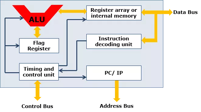

Computational Unit;
performs arithmetic and
logic operations

Various conditions of the
results are stored as
status bits called flags in
flag register

Internal storage of data

Generates the
address of the
instructions to be
fetched from the
memory and send
through address
bus to the
memory

Decodes instructions; sends
information to the timing and
control unit

Generates control signals for
internal and external
operations of the
microprocessor
Overview
3
8086 Microprocessor
First 16- bit processor released by
INTEL in the year 1978
Originally HMOS, now manufactured
using HMOS III technique
Approximately 29, 000 transistors, 40
pin DIP, 5V supply
Does not have internal clock; external
asymmetric clock source with 33%
duty cycle
20-bit address to access memory
can
address up to 2
20
= 1 megabytes of
memory space.
Pins and signals
Pins and Signals
5
8086 Microprocessor
Common signals
AD
0
-AD
15
(Bidirectional)
Address/Data bus
Low order address bus; these are
multiplexed with data.
When AD lines are used to transmit
memory address the symbol A is used
instead of AD, for example A
0
-A
15
.
When data are transmitted over AD lines
the symbol D is used in place of AD, for
example D
0
-D
7
, D
8
-D
15
or D
0
-D
15
.
A
16
/S
3
, A
17
/S
4
, A
18
/S
5
, A
19
/S
6
High order address bus. These are
multiplexed with status signals
Pins and Signals
6
8086 Microprocessor
Common signals
BHE (Active Low)/S
7
(Output)
Bus High Enable/Status
It is used to enable data onto the most
significant half of data bus, D
8
-D
15
. 8-bit
device connected to upper half of the
data bus use BHE (Active Low) signal. It
is multiplexed with status signal S
7
.
MN/ MX
MINIMUM / MAXIMUM
This pin signal indicates what mode the
processor is to operate in.
RD (Read) (Active Low)
The signal is used for read operation.
It is an output signal.
It is active when low.
Pins and Signals
7
8086 Microprocessor
Common signals
READY
This is the acknowledgement from the
slow device or memory that they have
completed the data transfer.
The signal made available by the devices
is synchronized by the 8284A clock
generator to provide ready input to the
8086.
The signal is active high.
Pins and Signals
8
8086 Microprocessor
Common signals
RESET (Input)
Causes the processor to immediately
terminate its present activity.
The signal must be active HIGH for at
least four clock cycles.
CLK
The clock input provides the basic timing
for processor operation and bus control
activity. Its an asymmetric square wave
with 33% duty cycle.
INTR Interrupt Request
This is a triggered input. This is sampled
during the last clock cycles of each
instruction to determine the availability
of the request. If any interrupt request is
pending, the processor enters the
interrupt acknowledge cycle.
This signal is active high and internally
synchronized.
Pins and Signals
9
8086 Microprocessor
Min/ Max Pins
The 8086 microprocessor can work in two
modes of operations :
Minimum mode
and
Maximum mode
.
In the
minimum mode
of operation the
microprocessor
do not
associate with any
co-processors and can not be used for
multiprocessor systems.
In the
maximum mode
the 8086
can work
in multi-processor or co-processor
configuration.
Minimum or maximum mode operations
are decided by the pin MN/ MX(Active low).
When this pin is
high
8086 operates in
minimum mode
otherwise it operates in
Maximum mode.
Pins and Signals
10
8086 Microprocessor
Minimum mode signals
Pins and Signals
11
8086 Microprocessor
Minimum mode signals
Pins and Signals
12
8086 Microprocessor
Maximum mode signals
Pins and Signals
13
8086 Microprocessor
Maximum mode signals
Pins and Signals
14
8086 Microprocessor
Maximum mode signals
Architecture
Architecture
16
8086 Microprocessor
Execution Unit (EU)
EU executes instructions that have
already been fetched by the BIU.
BIU and EU functions separately.
Bus Interface Unit (BIU)
BIU fetches instructions, reads data
from memory and I/O ports, writes
data to memory and I/ O ports.
Architecture
17
8086 Microprocessor
Bus Interface Unit (BIU)
Dedicated Adder to generate
20 bit address
Four 16-bit segment
registers
Code Segment (CS)
Data Segment (DS)
Stack Segment (SS)
Extra Segment (ES)
Segment Registers >>
Architecture
18
8086 Microprocessor
Bus Interface Unit (BIU)
Segment
Registers
•
8086’s 1-megabyte memory
is divided into segments of
up to 64K bytes each.
•
Programs obtain access to code
and data in the segments by
changing the segment register
content to point to the desired
segments.
•
The 8086 can directly address four
segments (256 K bytes within the 1
M byte of memory) at a particular
time.
Architecture
19
8086 Microprocessor
Bus Interface Unit (BIU)
Segment
Registers
Code Segment Register
•
16-bit
•
CS contains the base or start of the current code segment; IP contains the
distance or offset from this address to the next instruction byte to be fetched.
•
BIU computes the 20-bit physical address by logically shifting the contents of CS
4-bits to the left and then adding the 16-bit contents of IP.
•
That is, all instructions of a program are relative to the contents of the CS
register multiplied by 16 and then offset is added provided by the IP.
Architecture
20
8086 Microprocessor
Bus Interface Unit (BIU)
Segment
Registers
Data Segment Register
•
16-bit
•
Points to the current data segment; operands for most instructions are fetched
from this segment.
•
The 16-bit contents of the Source Index (SI) or Destination Index (DI) or a 16-bit
displacement are used as offset for computing the 20-bit physical address.
Architecture
21
8086 Microprocessor
Bus Interface Unit (BIU)
Segment
Registers
Stack Segment Register
•
16-bit
•
Points to the current stack.
•
The 20-bit physical stack address is calculated from the Stack Segment (SS) and
the Stack Pointer (SP) for stack instructions such as
PUSH
and
POP
.
•
In
based addressing mode
, the 20-bit physical stack address is calculated from
the
Stack segment (SS) and the
Base Pointer (BP).
Architecture
22
8086 Microprocessor
Bus Interface Unit (BIU)
Segment
Registers
Extra Segment Register
•
16-bit
•
Points to the extra segment in which data (in excess of 64K pointed to by the DS)
is stored.
•
String instructions use the ES and DI to determine the 20-bit physical address for
the destination.
Architecture
23
8086 Microprocessor
Bus Interface Unit (BIU)
Segment
Registers
Instruction Pointer
•
16-bit
•
Always points to the next instruction to be executed within
the currently executing code segment.
•
So, this register contains the 16-bit offset address pointing
to the next instruction code within the 64Kb of the code
segment area.
•
Its content is automatically incremented as the execution
of the next instruction takes place.
Architecture
24
8086 Microprocessor
Bus Interface Unit (BIU)
•
A group of First-In-First-Out (FIFO)
in which up to 6 bytes of
instruction code are pre fetched
from the memory ahead of time.
•
This is done in order to speed up
the execution by overlapping
instruction fetch with execution.
•
This mechanism is known as
pipelining
.
Instruction queue
Architecture
25
8086 Microprocessor
Some of the 16 bit registers can be
used as two 8 bit registers as :
AX can be used as AH and AL
BX can be used as BH and BL
CX can be used as CH and CL
DX can be used as DH and DL
Execution Unit (EU)
EU decodes and
executes instructions.
A decoder in the EU
control system
translates instructions.
16-bit ALU for
performing arithmetic
and logic operation
Four general purpose
registers(AX, BX, CX, DX);
Pointer registers (Stack
Pointer, Base Pointer);
and
Index registers (Source
Index, Destination Index)
each of 16-bits
Architecture
26
8086 Microprocessor
EU
Registers
Accumulator Register (AX)
•
Consists of two 8-bit registers AL and AH, which can be
combined together and used as a 16-bit register AX.
•
AL in this case contains the low order byte of the word,
and AH contains the high-order byte.
•
The I/O instructions use the AX or AL for inputting /
outputting 16 or 8 bit data to or from an I/O port.
•
Multiplication and Division instructions also use the AX or
AL.
Execution Unit (EU)
Architecture
27
8086 Microprocessor
EU
Registers
Base Register (BX)
•
Consists of two 8-bit registers BL and BH, which can be
combined together and used as a 16-bit register BX.
•
BL in this case contains the low-order byte of the word,
and BH contains the high-order byte.
•
This is the only general purpose register whose contents
can be used for addressing the 8086 memory.
•
All memory references utilizing this register content for
addressing use DS as the default segment register.
Execution Unit (EU)
Architecture
28
8086 Microprocessor
EU
Registers
Counter Register (CX)
•
Consists of two 8-bit registers CL and CH, which can be
combined together and used as a 16-bit register CX.
•
When combined, CL register contains the low order byte of
the word, and CH contains the high-order byte.
•
Instructions such as
SHIFT
,
ROTATE
and
LOOP
use the
contents of CX as a counter.
Execution Unit (EU)
Example:
The instruction
LOOP START
automatically decrements
CX by 1 without affecting flags and will check if [CX] =
0.
If it is zero, 8086 executes the next instruction;
otherwise the 8086 branches to the label START.
Architecture
29
8086 Microprocessor
EU
Registers
Execution Unit (EU)
Architecture
30
8086 Microprocessor
EU
Registers
Stack Pointer (SP) and Base Pointer (BP)
•
SP and BP are used to access data in the stack segment.
•
SP is used as an offset from the current SS during
execution of instructions that involve the stack segment in
the external memory.
•
SP contents are automatically updated (incremented/
decremented) due to execution of a POP or PUSH
instruction.
•
BP contains an offset address in the current SS, which is
used by instructions utilizing the based addressing mode.
Execution Unit (EU)
Architecture
31
8086 Microprocessor
EU
Registers
Source Index (SI) and Destination Index (DI)
•
Used in indexed addressing.
•
Instructions that process data strings use the SI and DI
registers together with DS and ES respectively in order to
distinguish between the source and destination addresses.
Execution Unit (EU)
Architecture
32
8086 Microprocessor
EU
Registers
Source Index (SI) and Destination Index (DI)
•
Used in indexed addressing.
•
Instructions that process data strings use the SI and DI
registers together with DS and ES respectively in order to
distinguish between the source and destination addresses.
Execution Unit (EU)
Memory Address Generation
33
34
•
The following examples shows the CS:IP scheme
of address formation:
35
Inserting a hexadecimal 0H (0000B)
with the CSR or shifting the CSR
four binary digits left
Architecture
36
8086 Microprocessor
Flag Register
Carry Flag
This flag is set, when there is
a carry out of MSB in case of
addition or a borrow in case
of subtraction.
Parity Flag
This flag is set to 1, if the lower
byte of the result contains even
number of 1’s ; for odd number
of 1’s set to zero.
Auxiliary Carry Flag
This is set, if there is a carry from the
lowest nibble, i.e, bit three during
addition, or borrow for the lowest
nibble, i.e, bit three, during
subtraction.
Zero Flag
This flag is set, if the result of
the computation or comparison
performed by an instruction is
zero
Sign Flag
This flag is set, when the
result of any computation
is negative
Tarp Flag
If this flag is set, the processor
enters the single step execution
mode by generating internal
interrupts after the execution of
each instruction
Interrupt Flag
Causes the 8086 to recognize
external mask interrupts; clearing IF
disables these interrupts.
Direction Flag
This is used by string manipulation instructions. If this flag bit
is ‘0’, the string is processed beginning from the lowest
address to the highest address, i.e., auto incrementing mode.
Otherwise, the string is processed from the highest address
towards the lowest address, i.e., auto incrementing mode.
Over flow Flag
This flag is set, if an overflow occurs, i.e, if the result of a signed
operation is large enough to accommodate in a destination
register. The result is of more than 7-bits in size in case of 8-bit
signed operation and more than 15-bits in size in case of 16-bit
sign operations, then the overflow will be set.
Execution Unit (EU)
37
Architecture
8086 Microprocessor
8086 registers
categorized
into 4 groups
38
Architecture
8086 Microprocessor
Registers and Special Functions
Memory
39
8086 Microprocessor
Memory
Processor Memory
Primary or Main Memory
Secondary Memory
Store Programs
and Data
Registers inside a microcomputer
Store data and results temporarily
No speed disparity
Cost
Storage area which can be directly accessed by
microprocessor
Store programs and data prior to execution
Should not have speed disparity with processor
Semi Conductor memories using CMOS technology
ROM, EPROM, Static RAM, DRAM
Storage media comprising of slow devices such as
magnetic tapes and disks
Hold large data files and programs: Operating
system, compilers, databases, permanent programs
etc.
Memory organization in 8086
40
8086 Microprocessor
Memory organization in 8086
41
8086 Microprocessor
The 8086 Microprocessor is a pivotal component in computer systems, with various functional blocks storing results as status bits called flags in the flag register. It performs arithmetic and logic operations, utilizes registers for data storage, features an ALU for generating addresses and instructions, and is equipped with a flag register, timing and control unit, and control buses. The 8086, released in 1978 by INTEL, operates in two modes and is distinguished by its pins and signals such as AD0-AD15, BHE, MN/MX, and RD.

Download Presentation

Please find below an Image/Link to download the presentation.
The content on the website is provided AS IS for your information and personal use only. It may not be sold, licensed, or shared on other websites without obtaining consent from the author.If you encounter any issues during the download, it is possible that the publisher has removed the file from their server.
You are allowed to download the files provided on this website for personal or commercial use, subject to the condition that they are used lawfully. All files are the property of their respective owners.
The content on the website is provided AS IS for your information and personal use only. It may not be sold, licensed, or shared on other websites without obtaining consent from the author.
E N D
Presentation Transcript
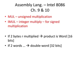
Microprocessor Functional blocks results are stored as status bits called flags in flag register Various conditions of the Computational performs arithmetic and logic operations Unit; Internal storage of data Register array or internal memory Data Bus ALU Generates address instructions to be fetched from the memory and send through bus to memory the the of Instruction decoding unit Flag Register address the Timing and control unit PC/ IP Address Bus Control Bus Generates control signals for internal and operations microprocessor Decodes information to the timing and control unit instructions; sends external of the 2
8086 Microprocessor Overview First 16- bit processor released by INTEL in the year 1978 Addressable organized in to two banks of 512 kb each; Even (or lower) bank and Odd (or higher) bank. Address line A0 is used to select even bank and control signal ??? is used to access odd bank memory space is Originally HMOS, now manufactured using HMOS III technique Uses a separate 16 bit address for I/O mapped devices can generate 216 = 64 k addresses. Approximately 29, 000 transistors, 40 pin DIP, 5V supply Operates in two modes: minimum mode and maximum mode, decided by the signal at MN and ?? pins. Does not have internal clock; external asymmetric clock source with 33% duty cycle 20-bit address to access memory address up to 220 = 1 megabytes of memory space. can 3
8086 Microprocessor Common signals Pins and Signals AD0-AD15 (Bidirectional) Address/Data bus Low multiplexed with data. order address bus; these are When AD lines are used to transmit memory address the symbol A is used instead of AD, for example A0-A15. When data are transmitted over AD lines the symbol D is used in place of AD, for example D0-D7, D8-D15 or D0-D15. A16/S3, A17/S4, A18/S5, A19/S6 High order address bus. These are multiplexed with status signals 5
8086 Microprocessor Common signals Pins and Signals BHE (Active Low)/S7 (Output) Bus High Enable/Status It is used to enable data onto the most significant half of data bus, D8-D15. 8-bit device connected to upper half of the data bus use BHE (Active Low) signal. It is multiplexed with status signal S7. MN/ MX MINIMUM / MAXIMUM This pin signal indicates what mode the processor is to operate in. RD (Read) (Active Low) The signal is used for read operation. It is an output signal. It is active when low. 6
8086 Microprocessor Common signals Pins and Signals TEST ???? input is tested by the WAIT instruction. 8086 will enter a wait state after execution of the WAIT instruction and will resume execution only when the ???? is made low by an active hardware. This is used to synchronize an external activity to the operation. processor internal READY This is the acknowledgement from the slow device or memory that they have completed the data transfer. The signal made available by the devices is synchronized by the 8284A clock generator to provide ready input to the 8086. 7 The signal is active high.
8086 Microprocessor Common signals Pins and Signals RESET (Input) Causes the processor to immediately terminate its present activity. The signal must be active HIGH for at least four clock cycles. CLK The clock input provides the basic timing for processor operation and bus control activity. Its an asymmetric square wave with 33% duty cycle. INTR Interrupt Request This is a triggered input. This is sampled during the last clock cycles of each instruction to determine the availability of the request. If any interrupt request is pending, the processor interrupt acknowledge cycle. enters the This signal is active high and internally synchronized. 8
8086 Microprocessor Min/ Max Pins Pins and Signals The 8086 microprocessor can work in two modes of operations : Minimum mode and Maximum mode. In the minimum mode of operation the microprocessor do not associate with any co-processors and can not be used for multiprocessor systems. In the maximum mode the 8086 can work in multi-processor configuration. or co-processor Minimum or maximum mode operations are decided by the pin MN/ MX(Active low). When this pin is high 8086 operates in minimum mode otherwise it operates in Maximum mode. 9
8086 Microprocessor Minimum mode signals Pins and Signals For minimum mode operation, the MN/ ?? is tied to VCC (logic high) Pins 24 -31 8086 itself generates all the bus control signals DT/ ? (Data Transmit/ Receive) Output signal from the processor to control the direction of data flow through the data transceivers (Data Enable) Output signal from the processor used as out put enable for the transceivers ??? ALE (Address Latch Enable) Used to demultiplex the address and data lines using external latches M/?? Used to differentiate memory access and I/O access. For memory reference instructions, it is high. For IN and OUT instructions, it is low. Write control signal; asserted low Whenever processor writes data to memory or I/O port ?? (Interrupt Acknowledge) When the interrupt request is accepted by the processor, the output is low on this line. ???? 10
8086 Microprocessor Minimum mode signals Pins and Signals For minimum mode operation, the MN/ ?? is tied to VCC (logic high) Pins 24 -31 8086 itself generates all the bus control signals HOLD Input signal to the processor form the bus masters as a request to grant the control of the bus. Usually used by the DMA controller to get the control of the bus. HLDA (Hold Acknowledge) Acknowledge signal by the processor to the bus master requesting the control of the bus through HOLD. The acknowledge is asserted high, when the processor accepts HOLD. 11
8086 Microprocessor Maximum mode signals Pins and Signals During maximum mode operation, the MN/ ?? is grounded (logic low) Pins 24 -31 are reassigned ??, ??, ?? Status signals; used by the 8086 bus controller to generate bus timing and control signals. These are decoded as shown. 12
8086 Microprocessor Maximum mode signals Pins and Signals During maximum mode operation, the MN/ ?? is grounded (logic low) Pins 24 -31 are reassigned ???, ??? (Queue Status) The processor provides the status of queue in these lines. The queue status can be used by external device to track the internal status of the queue in 8086. The output on QS0 and QS1 can be interpreted as shown in the table. 13
8086 Microprocessor Maximum mode signals Pins and Signals During maximum mode operation, the MN/ ?? is grounded (logic low) Pins 24 -31 are reassigned ??/???, ??/??? (Bus Request/ Bus Grant) These requests are used by other local bus masters to force the processor to release the local bus at the end of the processor s current bus cycle. These pins are bidirectional. The request on??? will have higher priority than??? An output signal activated by the LOCK prefix instruction. ???? Remains active until the completion of the instruction prefixed by LOCK. The 8086 output low on the executing an instruction prefixed by LOCK to prevent other bus masters from gaining control of the system bus. ???? pin while 14
8086 Microprocessor Architecture Execution Unit (EU) Bus Interface Unit (BIU) EU executes instructions that have already been fetched by the BIU. BIU fetches instructions, reads data from memory and I/O ports, writes data to memory and I/ O ports. BIU and EU functions separately. 16
8086 Microprocessor Bus Interface Unit (BIU) Architecture Dedicated Adder to generate 20 bit address Four 16-bit segment registers Code Segment (CS) Data Segment (DS) Stack Segment (SS) Extra Segment (ES) Segment Registers >> 17
8086 Microprocessor Bus Interface Unit (BIU) Architecture Segment Registers Programs obtain access to code and data in the segments by changing the segment register content to point to the desired segments. 8086 s 1-megabyte memory is divided into segments of up to 64K bytes each. The 8086 can directly address four segments (256 K bytes within the 1 M byte of memory) at a particular time. 18
8086 Microprocessor Bus Interface Unit (BIU) Architecture Code Segment Register Segment Registers 16-bit CS contains the base or start of the current code segment; IP contains the distance or offset from this address to the next instruction byte to be fetched. BIU computes the 20-bit physical address by logically shifting the contents of CS 4-bits to the left and then adding the 16-bit contents of IP. That is, all instructions of a program are relative to the contents of the CS register multiplied by 16 and then offset is added provided by the IP. 19
8086 Microprocessor Bus Interface Unit (BIU) Architecture Data Segment Register Segment Registers 16-bit Points to the current data segment; operands for most instructions are fetched from this segment. The 16-bit contents of the Source Index (SI) or Destination Index (DI) or a 16-bit displacement are used as offset for computing the 20-bit physical address. 20
8086 Microprocessor Bus Interface Unit (BIU) Architecture Stack Segment Register Segment Registers 16-bit Points to the current stack. The 20-bit physical stack address is calculated from the Stack Segment (SS) and the Stack Pointer (SP) for stack instructions such as PUSH and POP. In based addressing mode, the 20-bit physical stack address is calculated from the Stack segment (SS) and the Base Pointer (BP). 21
8086 Microprocessor Bus Interface Unit (BIU) Architecture Extra Segment Register Segment Registers 16-bit Points to the extra segment in which data (in excess of 64K pointed to by the DS) is stored. String instructions use the ES and DI to determine the 20-bit physical address for the destination. 22
8086 Microprocessor Bus Interface Unit (BIU) Architecture Instruction Pointer Segment Registers 16-bit Always points to the next instruction to be executed within the currently executing code segment. So, this register contains the 16-bit offset address pointing to the next instruction code within the 64Kb of the code segment area. Its content is automatically incremented as the execution of the next instruction takes place. 23
8086 Microprocessor Bus Interface Unit (BIU) Architecture Instruction queue A group of First-In-First-Out (FIFO) in which up to 6 bytes of instruction code are pre fetched from the memory ahead of time. This is done in order to speed up the execution by overlapping instruction fetch with execution. This mechanism is known as pipelining. 24
8086 Microprocessor Execution Unit (EU) Architecture EU decodes and executes instructions. A decoder in the EU control system translates instructions. 16-bit performing arithmetic and logic operation ALU for Four general purpose registers(AX, BX, CX, DX); Pointer registers (Stack Pointer, Base Pointer); and Some of the 16 bit registers can be used as two 8 bit registers as : Index registers (Source Index, Destination Index) each of 16-bits AX can be used as AH and AL BX can be used as BH and BL CX can be used as CH and CL DX can be used as DH and DL 25
8086 Microprocessor Execution Unit (EU) Architecture Accumulator Register (AX) EU Registers Consists of two 8-bit registers AL and AH, which can be combined together and used as a 16-bit register AX. AL in this case contains the low order byte of the word, and AH contains the high-order byte. The I/O instructions use the AX or AL for inputting / outputting 16 or 8 bit data to or from an I/O port. Multiplication and Division instructions also use the AX or AL. 26
8086 Microprocessor Execution Unit (EU) Architecture Base Register (BX) EU Registers Consists of two 8-bit registers BL and BH, which can be combined together and used as a 16-bit register BX. BL in this case contains the low-order byte of the word, and BH contains the high-order byte. This is the only general purpose register whose contents can be used for addressing the 8086 memory. All memory references utilizing this register content for addressing use DS as the default segment register. 27
8086 Microprocessor Execution Unit (EU) Architecture Counter Register (CX) EU Registers Consists of two 8-bit registers CL and CH, which can be combined together and used as a 16-bit register CX. When combined, CL register contains the low order byte of the word, and CH contains the high-order byte. Instructions such as SHIFT, ROTATE and LOOP use the contents of CX as a counter. Example: The instruction LOOP START automatically decrements CX by 1 without affecting flags and will check if [CX] = 0. If it is zero, 8086 executes the next instruction; otherwise the 8086 branches to the label START. 28
8086 Microprocessor Execution Unit (EU) Architecture Data Register (DX) EU Registers Consists of two 8-bit registers DL and DH, which can be combined together and used as a 16-bit register DX. When combined, DL register contains the low order byte of the word, and DH contains the high-order byte. Used to hold the high 16-bit result (data) in 16 X 16 multiplication or the high 16-bit dividend (data) before a 32 16 division and the 16-bit reminder after division. 29
8086 Microprocessor Execution Unit (EU) Architecture Stack Pointer (SP) and Base Pointer (BP) EU Registers SP and BP are used to access data in the stack segment. SP is used as an offset from the current SS during execution of instructions that involve the stack segment in the external memory. SP contents are automatically updated (incremented/ decremented) due to execution of a POP or PUSH instruction. BP contains an offset address in the current SS, which is used by instructions utilizing the based addressing mode. 30
8086 Microprocessor Execution Unit (EU) Architecture Source Index (SI) and Destination Index (DI) EU Registers Used in indexed addressing. Instructions that process data strings use the SI and DI registers together with DS and ES respectively in order to distinguish between the source and destination addresses. 31
8086 Microprocessor Execution Unit (EU) Architecture Source Index (SI) and Destination Index (DI) EU Registers Used in indexed addressing. Instructions that process data strings use the SI and DI registers together with DS and ES respectively in order to distinguish between the source and destination addresses. 32
Memory Address Generation Offset Value (16 bits) 0 0 0 0 Segment Register (16 bits) Adder Physical Address (20 Bits) 33
The following examples shows the CS:IP scheme of address formation: IP CS 34BA 8AB4 Code segment 34BA0 Inserting a hexadecimal 0H (0000B) 8AB4 (offset) with the CSR or shifting the CSR four binary digits left 3D654 3 4 B A 0 ( C S ) + 8 A B 4 ( I P ) 3 D 6 5 4 (next address) 44B9F 35
8086 Microprocessor Execution Unit (EU) Architecture This is set, if there is a carry from the lowest nibble, i.e, bit three during addition, or borrow for the lowest nibble, i.e, bit subtraction. Auxiliary Carry Flag Carry Flag Flag Register This flag is set, when there is a carry out of MSB in case of addition or a borrow in case of subtraction. three, during Zero Flag Parity Flag Sign Flag This flag is set, if the result of the computation or comparison performed by an instruction is zero This flag is set to 1, if the lower byte of the result contains even number of 1 s ; for odd number of 1 s set to zero. This flag is set, when the result of any computation is negative 15 14 13 12 11 10 9 8 7 6 5 4 3 2 1 0 OF DF IF TF SF ZF AF PF CF Tarp Flag Over flow Flag If this flag is set, the processor enters the single step execution mode by generating internal interrupts after the execution of each instruction This flag is set, if an overflow occurs, i.e, if the result of a signed operation is large enough to accommodate in a destination register. The result is of more than 7-bits in size in case of 8-bit signed operation and more than 15-bits in size in case of 16-bit sign operations, then the overflow will be set. Direction Flag Interrupt Flag This is used by string manipulation instructions. If this flag bit is 0 , the string is processed beginning from the lowest address to the highest address, i.e., auto incrementing mode. Otherwise, the string is processed from the highest address towards the lowest address, i.e., auto incrementing mode. Causes the 8086 to recognize external mask interrupts; clearing IF disables these interrupts. 36
8086 Microprocessor Architecture 8086 registers categorized into 4 groups 15 14 13 12 11 10 9 8 7 6 5 4 3 2 1 0 OF DF IF TF SF ZF AF PF CF Sl.No. Type Register width Name of register 1 General purpose register 16 bit AX, BX, CX, DX 8 bit AL, AH, BL, BH, CL, CH, DL, DH 2 Pointer register 16 bit SP, BP 3 Index register 16 bit SI, DI 4 Instruction Pointer 16 bit IP 5 Segment register 16 bit CS, DS, SS, ES 6 Flag (PSW) 16 bit Flag register 37
8086 Microprocessor Architecture Registers and Special Functions Register Name of the Register Special Function Stores the 16-bit results of arithmetic and logic operations AX 16-bit Accumulator Stores the 8-bit results of arithmetic and logic operations 8-bit Accumulator AL Used to hold base value in base addressing mode to access memory data BX Base register Used to hold the count value in SHIFT, ROTATE and LOOP instructions CX Count Register Used to hold data for multiplication and division operations DX Data Register Used to hold the offset address of top stack memory SP Stack Pointer Used to hold the base value in base addressing using SS register to access data from stack memory BP Base Pointer Used to hold index value of source operand (data) for string instructions SI Source Index Used to hold the index value of destination operand (data) for string operations DI Data Index 38
8086 Microprocessor Memory Processor Memory Registers inside a microcomputer Store data and results temporarily No speed disparity Cost Primary or Main Memory Storage area which can be directly accessed by microprocessor Store programs and data prior to execution Should not have speed disparity with processor Semi Conductor memories using CMOS technology ROM, EPROM, Static RAM, DRAM Memory Store Programs and Data Secondary Memory Storage media comprising of slow devices such as magnetic tapes and disks Hold large data files and programs: Operating system, compilers, databases, permanent programs etc. 39
8086 Microprocessor Memory organization in 8086 Memory IC s : Byte oriented 8086 : 16-bit Word : Stored by two consecutive memory locations; for LSB and MSB Address of word : Address of LSB Bank 0 : A0 = 0 memory bank Even addressed Bank 1 : ??? = 0 addressed memory bank Odd 40
8086 Microprocessor Memory organization in 8086 ??? Operation A0 Data Lines Used 1 Read/ Write byte at an even address 1 0 D7 D0 2 Read/ Write byte at an odd address 0 1 D15 D8 3 Read/ Write word at an even address 0 0 D15 D0 4 Read/ Write word at an odd address 0 1 D15 D0 in first operation byte from odd bank is transferred 1 0 D7 D0 in first operation byte from odd bank is transferred 41