Solid State Chemistry: Amorphous vs. Crystalline Solids
Solid state chemistry involves studying the differences between amorphous and crystalline solids, exploring their unique properties such as melting points, isotropic/anisotropic characteristics, and examples of each type of solid. Additionally, the classification of crystals into different crystal systems based on their shapes and Bravais lattices, along with details on closed packed structures like hcp and ccp, are discussed in detail.

Download Presentation

Please find below an Image/Link to download the presentation.
The content on the website is provided AS IS for your information and personal use only. It may not be sold, licensed, or shared on other websites without obtaining consent from the author.If you encounter any issues during the download, it is possible that the publisher has removed the file from their server.
You are allowed to download the files provided on this website for personal or commercial use, subject to the condition that they are used lawfully. All files are the property of their respective owners.
The content on the website is provided AS IS for your information and personal use only. It may not be sold, licensed, or shared on other websites without obtaining consent from the author.
E N D
Presentation Transcript
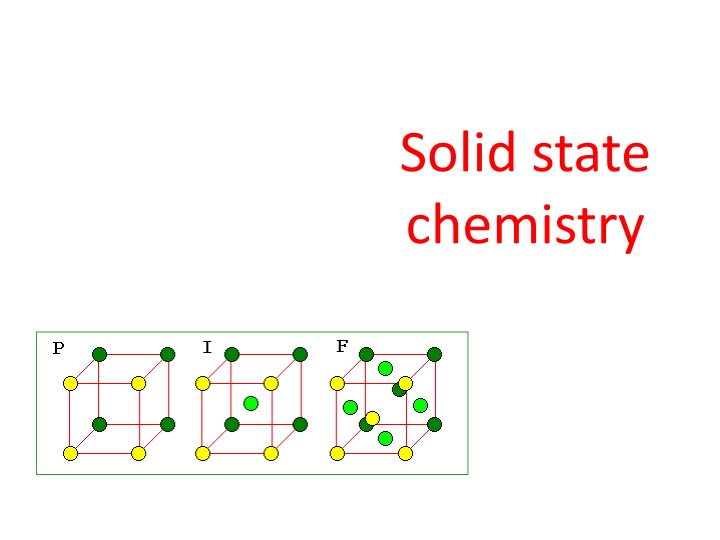
Solid state chemistry
Difference Between Amorphous and Crystalline Solids Amorphous Crystalline Amorphous without form) are the solids which lacks arrangement molecules and hence they have a short range order or no order in their ABCBBACBCACCB... Do not have sharp melting point (because all bonds are not equally strong) Isotropic (Physical properties are same different directions) Examples: glass, wax, plastics, etc. A crystalline solid is the one in which there repeating pattern structure, or in other words, there is long-range order : ABCABCABCABC Have sharp (because all bond are equally strong) Anisotropic properties are different in different directions) Examples: diamond, table salt, ice, methanol, chloride, etc. solids (means is a regular in the regular the of atoms or structure : melting point (Physical in sodium
CRYSTAL SYSTEMS AND BRAVAIS LATTICES Crystals of different substances have similar shapes and hence the crystals are classified into the so called crystal systems depending upon their axial ratio and the interfacial angles , and . In three- dimension, there are 7 crystal systems. Bravais showed that throughout the seven crystal systems there are fourteen unique lattice types possible. These are known as Bravais or space lattices. These seven crystal systems with examples are : Cubic(CsCl, NaCl, Cu) Tetragonal(SnO2) Orthorhombic(PbSO4, MgSO4) Monoclinic(FeSO4, LiSO4 H2O) Triclinic(FeSO4 5H2O, K2Cr2O7) Trigonal (Rhombohedral)(Sb, As, CaCO3) Hexagonal(Zn, Cd, Ni, As, SiO2) The characteristics features of these crystal systems and the corresponding Bravais lattices are as follows:
No. Crystal class Intercepts Angles between Axes = = = 900 Bravais space lattice on Axes a = b = c 1 Cubic Simple, body-centred, face-centred Simple, body-centred a = b c = = = 900 2 Tetragonal Orthorhombic a b c = = = 900 3 Simple, body-centred, face-centred, Base(side)-centred Simple a = b = c = = 900 4 Trigonal a = b c = = 900, = 1200 = = 900 5 Hexagonal Simple a b c a b c 6 7 Monoclinic Triclinic Simple, base-centred Simple
Closed Packed Structures In a closed packed structure the constituent atoms are so arranged as to occupy minimum possible volume, reaching the maximum density. 2-layers closed packed structure Planar closed packed spheres
Closed Packed Structures hcp ccp Hexagonal Closed Packed Cubic Closed Packed
Closed Packed Structures hcp ccp Hexagonal Closed Packed Cubic Closed Packed
c.c.p. structure (111) Of a FCC structure
MILLER INDICES The crystal structure may be regarded as made up of an aggregate of a set of parallel equidistant planes passing through at least one lattice point or a number of lattice points. These planes are known as Lattice Planes. For a given crystal, lattice planes can be chosen in different ways as shown in Fig. Miller Indices are the three smallest possible integers, which have the same ratio as the reciprocals of intercepts of the plane concerned on the three axis.
INTERPLANER DISTANCE OR SPACING Interplaner spacing is defined as the perpendicular distance dhkl between corresponding planes. It is also perpendicular distance from the origin to the set of parallel planes (see Fig.)
2 2 2 a b c 2 = + + dhkl 2 2 2 h k l For a cubic lattice, a = b = c, therefore, we get dhkl a = + + 2 2 2 h k l Also, For a cubic lattice, d100= a d110= a/ 2 d111= a/ 3.
Physical Parameters for Crystal Structure (i) Number of Atoms per Unit Cell Number of atoms per unit cell determines how closely the solid is packed and is given by N = Nc/8 + Nf/2 + Ni here Ncis the number of corner atoms, Nfthe number of face centred atoms and Nithe number of body centred atoms(see Fig.). For SC crystal : In a SC crystal, there are 8 atoms only, each at one corner. Each atom is shared by 8 unit cells. Therefore, we have N = Nc/8 = 8/8 = 1 For BCC crystal :N = Nc/8 + Nf/2 + Ni= 8/8 + 0 + 1 = 2 For FCC crystal :N = Nc/8 + Nf/2 + Ni= 8/8 + 6/2 + 0 = 4
(ii) Coordination Number (CN) In a crystal, the number of nearest neighbours of the same type and at equal distances from the given atom is called coordination number. For SC : The corner atoms are the nearest neighbours of each other. Here CN = 6 (see Fig.) which is a group of 8 unit cell and atom at the centre has six corner atoms as its nearest neighbours).
For BCC : distances from the body centered atom. Hence CN = 8. In this case all the corner atoms are at equal For FCC : Here the nearest neighbours of any corner atom are the face centered atoms of the surrounding unit cells. Now for any corner atom there are 4 face centered atoms in each plane and there are three such planes. Therefore, CN = 12.
(iii) Atomic Radius and Nearest Neighbour Distance (NND) In a crystal the atoms are assumed to be spheres in contact. Now atomic radius is defined as half the distance between the nearest neighbours in a crystal of pure element, i.e., the distance between the centres of neighbouring atoms. For SC : In a SC structure, corner atoms are the nearest neighbours and are in touch with each other. If the side of the unit cell is a and r be the radius , then 2r = a or Now Nearest Neighbour Distance(NND) is given by 2r Therefore, NND = 2r = a r = a/2
r = 2 a/4 For FCC : NND = a/ 2
r = 3 a/4 NND = 3 a/2. For BCC :
(iv) Atomic Packing Fraction (or Factor) (APF) It is defined as the ratio of the volume of the atoms occupying the unit cell to the volume of the unit cell. It is also called relative packing density. APF = Volume occupied by the atoms in a unit cell / Volume of the unit cell. SC Crystal : No. of atoms/unit cell = 1 Volume of one atom = 4/3 r3 Side of the unit cell = a = 2r Volume of the unit cell = a3 APF = = = /6 = 0.52 = 52%. BCC Crystal : No. of atoms/unit cell = 2 Volume of two atoms = 2x4/3 r3 Side of the unit cell = a = 4r/ 3 Volume of the unit cell = a3 APF = = = 3 /8 = 0.68 = 68%. FCC Crystal : No. of atoms/unit cell = 4 Volume of four atoms = 4x4/3 r3 Side of the unit cell = a = 4r/ 2 Volume of the unit cell = a3 APF = = = 2 /6 = 0.74 = 74%.
Interstitial sites in Closed Packed Structures Having determined what types of interstitial sites are available, we must now decide: (a) Which sites are occupied by a given cation: this determined by the radius ratio (= rcation/ranion) (b) How many sites are occupied: this is determined by the stoichiometry. For an octahedral site: For a tetrahedral site, rcation/ranion= 0.225. For these two values, the close packed structure of anions is maintained.
Interstitial sites in Closed Packed Structures Stable Bonding Configurations in Ionic solids. In reality an ideal fit of a cation into the close packed anion arrangement almost never occurs. Now consider what would be the consequence of placing a cation that is (a) larger than the ideal, (b) smaller than the ideal, into the cation sites. For a stable coordination the bonded cation and anion must be in contact with each other. If rcation/ranionbecomes too big, the close packed structure of anions is converted into a simple cubic structure
Rock salt structure rNa= 0.102 nm rCl= 0.181 nm rNa/rCl= 0.564 Octahedral sites preferred
Zinc blende structure Zn 2+ S 2- rZn/rS= 0.40 tetrahedral sites preferred
Fluorite and antifluorite Calcium Fluorite (CaF2) Cations in cubic sites UO2,ThO2, ZrO2, CeO2 Antifluorite structure positions of cations and anions reversed Fluorite structure rCa/rF= 0.958 cubic sites preferred
Perovskite ABO3 Perovskite structure Ex: complex oxide BaTiO3
Spinels Normal Inverse
Spinels Normal Inverse In order to explain the adoption of a particular cation distribution in a spinel structure, one must take into account the crystal field stabilization energies (CFSE) of the transition metals present. Some ions may have a distinct preference for the octahedral site depending on the d-electron count. If the A2+ions have a strong preference for the octahedral site, they will displace half of the B3+ions from the octahedral sites to tetrahedral sites. Similarly, if the B3+ions have a low or zero octahedral site stabilization energy (OSSE), then they will occupy tetrahedral sites, leaving octahedral sites for the A2+ions.
DEFECTS IN SOLIDS No real crystal is perfect. Real crystals feature defects or irregularities in their ideal arrangements and it is these defects that critically determine many of the electrical and mechanical properties of real materials. Ideally a perfect crystal is the one in which atoms are arranged in perfectly regular manner in all directions. The deviations of crystals from their perfect periodicity are called defects or imperfections. These imperfections can be of different types such as: point defects (zero dimensional defects), line defects (one dimensional) defects over a surface or a plane (two dimensional) and volume defects (three dimensional).
Point Defects A point defect is a very localized imperfection in the regularity of a lattice and it does not spread over more than one or two lattice spacings. These defects are observed in metallic crystals (vacancies, substitutional impurity and interstitials) as well as in ionic crystals (Schottky and Frenkel) and are discussed here in brief. Vacancies The absence of an atom or ion from a normally occupied site in a crystal is called a vacancy (see Fig.) Substitutional Impurity In this kind of defect, a foreign atom occupy a regular site in the crystal structure (see Fig.), i.e., .substitutional atom replaces the host atom from its position. For example, when a pure semiconductor crystal of Silicon or Germanium is doped with a trivalent or pentavalent impurity, we call it a substitutional impurity.
Interstitial Impurity An interstitial is an atom or ion which can be inserted into the voids between the regularly occupied sites. In a closed packed arrangement of atoms the packing fraction is generally less than one. Therefore an extra atom, of smaller size than the parent atom, can enter the interstitial space without disturbing the regularly positioned atoms. Such an extra impure atom is called interstitial impurity while an extra atom in an interstitial position is called self interstitial atom, as shown in Fig. If the size of the extra atom is not small then it will produce atomic distortion.
Schottky Defect In a metal, a vacancy is created if an atom is missing from its lattice position. In ionic crystals, a cation anion pair will be missing from the respective lattice sites, as shown in Fig. Creation of such a pair, of one cation vacancy together with one anion vacancy, is called Schottky defect. Thus the interior of the ionic crystals remain electrically neutral. Frenkel Defect When an atom or ion leaves its normal position or site and is found to occupy another position in the interstice we get a Frenkel defect. Thus, in this case, two imperfections are created an interstitial and a vacancy as shown in Fig. Normally anion leaves its parent site and occupy the interstitial space. These defects are dominant in open structures such as silver halides. Also a Frenkel defect does not affect the electrical neutrality of a crystal.
Shottky defect E = n Ne 2 kT n = number of vacancy pairs N = total number of sites E = energy required to produce a pair of vacancies in the interior of a crystal
Frenkel defect E 1 i = ( ) n N N e 2 kT 2 i n = number of vacancies = number of atoms in interstitial sites N = total number of sites Ni= number of interstitial positions in the crystal Ei= energy required to produce a pair of vacancies in the interior of a crystal
Emerald and Ruby: Cr3+impurities Cr2O3: green
D DO1 Cr-O distance in Be3Al2(SiO3)6 is larger than in Al2O3 D DO1 < D DO2 D DO2
Charge compensation: vacancy formation When a divalent cation replaces a monovalent cation, a second monovalent cation must also be removed, creating a vacancy.
Charge compensation: change in oxidation state When a divalent cation replaces a monovalent cation, an anion must change its oxidation state.
Electronic properties of materials Justify: - Electron transport properties - Optical properties


 Coordination Number (CN)")

 Atomic Radius and Nearest Neighbour Distance (NND)")


 Atomic Packing Fraction (or Factor) (APF)")


 2003 Brooks/Cole Publishing / Thomson Learning")