Planar Transmission Lines: A Comprehensive Overview
Exploring various planar transmission lines like Microstrip, Stripline, Coplanar Waveguide, and Slotline. Understanding the field structures, analysis complexities, and solutions using conformal mapping in Stripline designs. Detailed discussions on characteristic impedance and effective width calculations.

Download Presentation

Please find below an Image/Link to download the presentation.
The content on the website is provided AS IS for your information and personal use only. It may not be sold, licensed, or shared on other websites without obtaining consent from the author.If you encounter any issues during the download, it is possible that the publisher has removed the file from their server.
You are allowed to download the files provided on this website for personal or commercial use, subject to the condition that they are used lawfully. All files are the property of their respective owners.
The content on the website is provided AS IS for your information and personal use only. It may not be sold, licensed, or shared on other websites without obtaining consent from the author.
E N D
Presentation Transcript
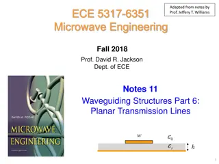
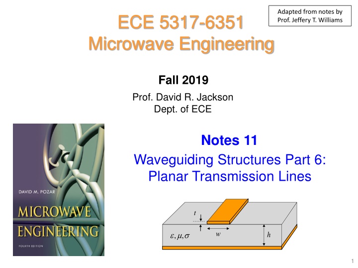
Adapted from notes by Prof. Jeffery T. Williams ECE 5317-6351 Microwave Engineering Fall 2019 Prof. David R. Jackson Dept. of ECE Notes 11 Waveguiding Structures Part 6: Planar Transmission Lines t w , , h 1
Planar Transmission Lines w w b r h r Microstrip Stripline w w r r g g h g g h Coplanar Waveguide (CPW) Conductor-backed CPW s s r r h h Slotline Conductor-backed Slotline 2
Planar Transmission Lines (cont.) w w w w r h r s h s Coplanar Strips (CPS) Conductor-backed CPS Stripline is a planar version of coax. Coplanar strips (CPS) is a planar version of twin lead. 3
Stripline Common on circuit boards t Fabricated with two circuit boards w b , , Homogenous dielectric (perfect TEM mode*) TEM mode * The mode is a perfect TEM mode if there is no conductor loss. (also TE & TM Modes at high frequency) Field structure for TEM mode: Electric Field Magnetic Field 4
Stripline (cont.) Analysis of stripline is not simple. TEM mode fields can be obtained from an electrostatic analysis (e.g., conformal mapping). A closed stripline structure is analyzed in the Pozar book by using an approximate numerical method: b w / 2 b , , a a b (to simulate stripline) 5
Stripline (cont.) Conformal Mapping Solution (R. H. T. Bates) Exact solution (for t = 0): K k 30 ( ) = Z K= complete elliptic integral of the first kind 0 ( ) K k /2 1 ( ) K k d 2 2 1 sin k 0 w b w b = sech k 2 R. H. T. Bates, The characteristic impedance of the shielded slab line, IEEE Trans. Microwave Theory and Techniques, vol. 4, pp. 28-33, Jan. 1956. = tanh k 2 6
Stripline (cont.) Curve fitting this exact solution: b = Z ( ) 0 ln 4 ln(4) 0 = Note: 0.441 4 + w b r e Fringing term Effective width w b 0 ; 0.35 for w b w b = e 2 w b w b 0.35 ; 0.1 0.35 for 1 2 / 2 w b b b w Note: = = = ideal 0 The factor of 1/2 in front is from the parallel combination of two ideal PPWs. 0 Z 4 4 w r 7
Stripline (cont.) Inverting this solutionto find w for given Z0: ; 120 X Z for 0 r w b = 0.85 0.6 ; 120 X Z for 0 r ln(4) X 0 4 Z 0 r 8
Stripline (cont.) Attenuation Dielectric Loss: k k = 0 r tan tan k (TEM formula) d d d 2 2 c j = = = = k k jk tan 0 c d c c sR t sR b w , , sR 9
Stripline (cont.) Conductor Loss: 4 R Z ( ) (2.7 10 ) 3 ; 120 0 ) s b t r A Z wider strips fo r 0 r ( 0 c R Z b ( ) 0.16 ; 120 s B Z narrower strips for 0 r 0 = sR 2 wher e = conductivity of metal + 1 2 w b t b t b t t 1 2 = + + ln A ( ) b t 1 2 1 b t w w t = + + + + 1 0.414 ln 4 B w 2 + 0.7 t 2 Note: We cannot let t 0 when we calculate the conductor loss. 10
Stripline (cont.) Note about conductor attenuation: It is necessary to assume a nonzero conductor thickness in order to accurately calculate the conductor attenuation. The perturbational method predicts an infinite attenuation if a zero thickness is assumed. (0) 2 P P = l c 1 = 0 0: 0 t J s as sz s R 2 = (0) P J d s l s 2 + C C = 0 z 1 2 ( ) J on strip sz Practical note: A standard metal thickness for PCBs is 0.7 [mils] (17.5 [ m]), called half-ounce copper . t s b r w 1 mil = 0.001 inch 11
Microstrip t w , , h Inhomogeneous dielectric No TEM mode Note: Pozar uses (W, d) TEM mode would require kz = kin each region, but kz must be unique! Requires advanced analysis techniques Exact fields are hybrid modes (Ezand Hz) For h / 0 << 1, the dominant mode is quasi-TEM. 12
Microstrip (cont.) Part of the field lines are in air, and part of the field lines are inside the substrate. Figure from Pozar book Note: The flux lines get more concentrated in the substrate region as the frequency increases. 13
Microstrip (cont.) Equivalent TEM problem: Actual problem eff r k 0 w 0 r 2 h = eff r k 0 The effective permittivity gives the correct phase constant. The effective strip width gives the correct Z0. r eff Z eff w 0 h = air eff r 0/ Z Z 0 Equivalent TEM problem ( ) = since / Z L C 0 14
Microstrip (cont.) Effective permittivity: Note: + This formula ignores dispersion , i.e., the fact that the effective permittivity is actually a function of frequency. 1 1 1 = + eff r r r 2 2 h w 1 12 + Limiting cases: + 1 eff r / 0: w h r (narrow strip) 2 eff r / : w h (wide strip) w 0 r r h 15
Microstrip (cont.) Characteristic Impedance: 60 8 w h w h w h + ln ; 1 for 4 eff r = Z w h 0 ; 1 0 for w h w h + 1.393 0.667ln + + eff r 1.444 Note: This formula ignores the fact that the characteristic impedance is actually a function of frequency. 16
Microstrip (cont.) Inverting this solution to find w for a given Z0: A 8 A e w h ; 2 for 2 2 e w h = 2 1 0.61 w h ( ) 1 ln(2 + + 1) ln 1 0.39 ; 2 B B B r for 2 r r where + + 1 1 1 0.11 Z = + + 0.33 A 0 r r 60 2 r r = B 0 2 Z 0 r 17
Microstrip (cont.) More accurate formulas for characteristic impedance that account for dispersion (frequency variation) and conductor thickness: ( ) ( ) 0 ( ) ( ) f eff r eff r eff r eff r 1 1 0 f ( ) f ( ) 0 = Z Z 0 0 ( ) = 00 Z 0 ( / w h 1) ( ) ( ) ( 0 ) ( ) w h w h + 1.393 0.667ln + + eff r / / 1.444 2 t h t = + 1 ln + w w w t r h 18
Microstrip (cont.) where 2 eff r (0) ( / w h ( ) f 1) = + r eff r eff r (0) 1.5 1 4 + F + 1 1 1 1 / t h w h ( ) 0 = + eff r r r r ( ) 2 2 4.6 1 12 + / / h w 2 0: f h w h As = + 1 0.868ln 1 + + 1 0.5 4 F Note: ( ) r ( ) 0 eff r eff r f 0 : f As w t ( ) f eff r r r h 19
Microstrip (cont.) 2 = eff r Effective dielectric constant k 12.0 0 r 11.0 c = v 10.0 p eff r 9.0 Frequency variation (dispersion) A frequency-dependent solution for microstrip transmission lines," E. J. Denlinger, IEEE Trans. Microwave Theory and Techniques, Vol. 19, pp. 30-39, Jan. 1971. 8.0 7.0 Frequency (GHz) Parameters: r = 11.7, w/h = 0.96, h = 0.317 cm Note: The flux lines get more concentrated in the substrate region as the frequency increases. Note: The phase velocity is a function of frequency, which causes pulse distortion. Quasi-TEM region 20
Microstrip (cont.) Attenuation Dielectric loss: filling factor ( ) eff r 1 k 0 r tan r ( ) d d eff r 2 1 r eff r 1: 0 d Conductor loss: k eff r 0 r : tan R R r d d 2 s s c Z w h 0 very crude ( parallel-plate ) approximation (More accurate formulas are given on next slide.) h Z 0 w 21
Microstrip (cont.) More accurate formulas for conductor attenuation: 2 1 w h 1 2 R hZ w h w h w h t t h = + + 2 1 1 ln s c 2 4 h 2 0 ( ) 2 / w w h w h 2 2 R hZ w h w w h h w h w h t t h = + + + + + ln 2 0.94 1 ln e s 2 c 2 h + 0.94 0 2 h This is the number e = 2.71828 multiplying the term in parenthesis. 2 t h t = + 1 ln + w w w t r h 22
Microstrip (cont.) REFERENCES L. G. Maloratsky, Passive RF and Microwave Integrated Circuits, Elsevier, 2004. I. Bahl and P. Bhartia, Microwave Solid State Circuit Design, Wiley, 2003. R. A. Pucel, D. J. Masse, and C. P. Hartwig, Losses in Microstrip, IEEE Trans. Microwave Theory and Techniques, pp. 342-350, June 1968. R. A. Pucel, D. J. Masse, and C. P. Hartwig, Corrections to Losses in Microstrip , IEEE Trans. Microwave Theory and Techniques, Dec. 1968, p. 1064. 23
TXLINE This is a public-domain software for calculating the properties of some common planar transmission lines. https://www.awr.com/software/options/tx-line 24


")

")
")
")
")
")
")
")

")
")
")
")
")
")
")
")
")
")
")