Extrinsic Semiconductors: Fermi Level and Doping Effects
Extrinsic semiconductors play a crucial role in modern electronics by allowing controlled addition of impurities to tailor conductivity. The Fermi level in extrinsic semiconductors shifts based on the number of electrons and holes in the conduction and valence bands, influencing conductivity. Doping with specific impurities like Group V and III elements modifies charge concentration, affecting semiconductor behavior. N-type semiconductors, with pentavalent impurities, have excess electrons in the conduction band, while p-type semiconductors, with trivalent impurities, have excess holes in the valence band. Understanding these principles is vital for semiconductor device design and fabrication.

Download Presentation

Please find below an Image/Link to download the presentation.
The content on the website is provided AS IS for your information and personal use only. It may not be sold, licensed, or shared on other websites without obtaining consent from the author.If you encounter any issues during the download, it is possible that the publisher has removed the file from their server.
You are allowed to download the files provided on this website for personal or commercial use, subject to the condition that they are used lawfully. All files are the property of their respective owners.
The content on the website is provided AS IS for your information and personal use only. It may not be sold, licensed, or shared on other websites without obtaining consent from the author.
E N D
Presentation Transcript
Course Code: MSE-S303 Electronic and Optical Materials LECTURE 3 Fermi level and Effect of temperature on Extrinsic Semiconductors Faculty Name : Dr.Anju Dixit MSME Department UIET CSJM University Kanpur 1
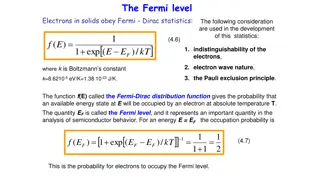
Recap The Fermi energy is a concept in quantum mechanics usually referring to the energy of the highest occupied quantum state in a system of fermions at absolute zero temperature. The Fermi-Dirac distribution, also called the "Fermi function," is a fundamental equation expressing the behaviour of mobile charges in solid materials In intrinsic SC the number of electrons is equal to the number of holes (ni=pi) and Fermi level is at the centre of the forbidden gap. For intrinsic SC as the temperature increases both ni and pi will increase and Fermi level will remain approximately at the center of the forbidden gap. This means Fermi level is independent of the temperature 2
Doping in Semiconductor Deliberate addition of impurities in a controlled way allows tailoring of charge concentration and hence conductivity to desired values. Process is referred to as doping essential for device fabrication. Doped semiconductors referred to as extrinsic. Most important impurities (dopants) are from: Group V in Periodic Table e.g. P, As Group III in Periodic Table e.g. B, Al 3
Fermi level of extrinsic semiconductor In extrinsic semiconductor, the number of electrons in the conduction band and the number of holes in the valence band are not equal. Hence, the probability of occupation of energy levels in conduction band and valence band are not equal. Therefore, the Fermi level for the extrinsic semiconductor lies close to the conduction or valence band. in n-type SC, number of electrons ne>ni and number of holes pe<pi This means ne>pe , hence the Fermi level must move upward closer to the conduction band For p-type SC, pe>ne so Fermi level must move downward from the center of the forbidden gap closer to the valence band 4
N-type Semiconductor In n-type semiconductor pentavalent impurity is added. Each pentavalent impurity donates a free electron. The addition of pentavalent impurity creates large number of free electrons in the conduction band At room temperature, the number of electrons in the conduction band is greater than the number of holes in the valence band. Extra Electron energy levels Hence, the probability of occupation of energy levels by the electrons in the conduction band is probability of occupation of energy levels by the holes in the valence band. greater than the This probability of occupation of energy levels is represented in terms of Fermi level. Therefore, the Fermi level in the n-type semiconductor lies close to the conduction band. 5
P-type Semiconductor In p-type semiconductor trivalent impurity is added. Each trivalent impurity creates a hole in the valence band and ready to accept an electron. The addition of trivalent impurity creates large number of holes in the valence band. At room temperature, the number of holes in the valence band is greater than the number of electrons in the conduction band. Hence, the probability of occupation of energy levels by the holes in the valence band is greater than the probability of occupation of energy levels by the electrons in the conduction band. Extra Hole energy levels This probability of occupation of energy levels is represented in terms of Fermi level. Therefore, the Fermi level in the p-type semiconductor lies close to the valence band. 6
Conduction in N and P type semiconductors In an N type semiconductor, the current flows due to the movement of free electrons and holes. Since the free electrons being the majority carriers and holes being the minority carriers, the net current will be due to the majority carriers i.e. free electrons. In a P type semiconductor, the current flows due to the movement of holes and free electrons. Since hole being the majority carriers and free elctrons beimg the minority carriers, the net current will be due to the majority carriers i.e. the holes. 7
Energy Bands of Extrinsic Semiconductors In extrinsic semiconductors, a change in the ambient temperature leads to the production of minority charge carriers. Also, the dopant atoms produce the majority carriers. During recombination, the majority carriers destroy most of these minority carriers. This leads to a decrease in the concentration of the minority carriers. Therefore, this affects the energy band structure of the semiconductor. In such semiconductors, additional energy states exist: Energy state due to donor impurity (ED) Energy state due to acceptor impurity (EA) 8
N-type Semiconductor If we consider the most common and preferred n-type dopant, phosphorus, it has the tendency to loose its fifth electron in the semiconductor onto the conduction band when it gets some external energy. Initially, (at 0K) the loosely held electron is still in control of the nucleus of donor atom. This is due to the bind energy of the atom, which is the energy required to bind the electron with the atom. Since, a donor atom can be approximated as a hydrogen atom (tendency to give only one electron), its bind energy comes out to be less than 0.1eV ! Meaning, that much energy is sufficient to ionize the donor. Hence, as a result, donor level adjust itself only that much far from conduction band, which is very small energy gap. The same thought can be incorporated for acceptor level. 9
Energy Bands of N-type Semiconductors The energy level of the donor (ED) is lower than that of the conduction band (EC). At 0 K all allowed energy levels in the valence band are filled by electrons. Donor levels are filled by unbound electrons. Hence, electrons can move into the conduction band with minimal energy (~0.01 eV). Also, at room temperature, most donor atoms and very few Si atoms get ionized. Hence, the conduction band has most electrons from the donor impurities. 10
Energy Bands of P-type Semiconductors The energy level of the acceptor (EA) is higher than that of the valence band (EV). Hence, electrons can move from the valence band to the level EA, with minimal energy. Also, at room temperature, most acceptor atoms are ionized. At absolute zero, all the holes are in acceptor levels, but as the temperature rises, the electrons from valence band jump into acceptor level on the absorption of energy (Ea-Ev) by each electron. At the room temperature, almost all acceptor atoms trap electrons and thus the number of holes available in the valence band is almost equal to the number of impurity atoms added. As a result, these electrons are trapped in the acceptor levels and an equal number of holes are created in the valence band. 11
N-Type Semiconductor at High Temperature N-type semiconductor the Fermi-level lies below the bottom of the conduction band. As temperature rises, the Fermi level goes on falling below E C . As temperature is sufficiently raised, the electrons and holes generated due to thermal agitation increase significantly and at a stage intrinsic become fully dominant over the extrinsic carriers. Then the Fermi level approaches the middle of forbidden energy gap. 12
P-Type Semiconductor at High Temperature Fermi level lies above the top of the valence band. The position of Fermi level depends upon the temperature and then number of impurity atoms. As the temperature is sufficiently increased, electrons from the valence band are excited to the conduction band and finally the P-type crystal will start behaving like an intrinsic semi-conductor when the number of electrons in the conduction band will be nearly equal to the valence holes. Thus at extremely high temperatures the Fermi level shifts towards the middle of forbidden energy gap. 13
Summary In N-type semiconductor the Fermi-level lies below the bottom of the conduction band. In P-type Semiconductor the Fermi level lies above the top of the valence band. The position of Fermi level in both cases depends upon the temperature and then number of impurity atoms. At very high temperatures the Fermi level approaches the middle of forbidden energy gap, hence behave like Intrinsic semiconductor in both N and P type semiconductors. 14