Innovative Applications of Associative Memory in Modern Electronic Devices
Explore the diverse applications of combining FPGA with specific ASICs and associative memories in smart systems, error decoding, image processing, advertising displays, and workplace monitoring. Learn about Content Addressable Memory (CAM) utilization, pattern matching techniques, and real-life examples showcased at the WASC14 Conference. Discover how this technology can be harnessed for tasks like genetic code decoding and smart camera operations.

Download Presentation

Please find below an Image/Link to download the presentation.
The content on the website is provided AS IS for your information and personal use only. It may not be sold, licensed, or shared on other websites without obtaining consent from the author.If you encounter any issues during the download, it is possible that the publisher has removed the file from their server.
You are allowed to download the files provided on this website for personal or commercial use, subject to the condition that they are used lawfully. All files are the property of their respective owners.
The content on the website is provided AS IS for your information and personal use only. It may not be sold, licensed, or shared on other websites without obtaining consent from the author.
E N D
Presentation Transcript
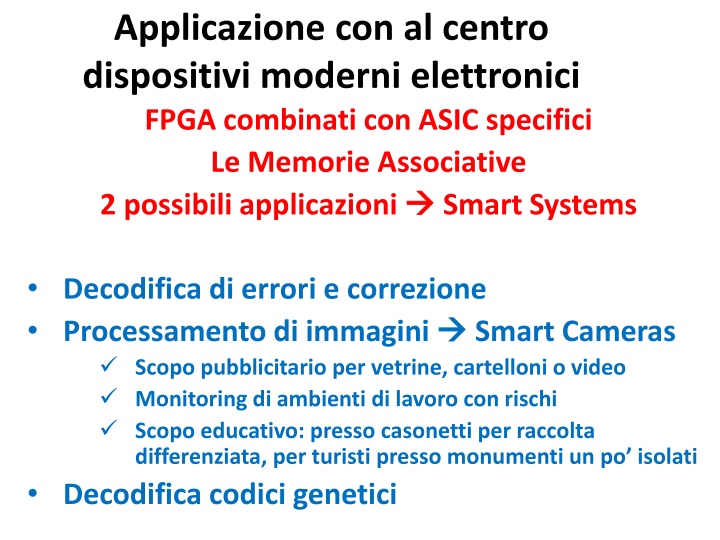
Applicazione con al centro dispositivi moderni elettronici FPGA combinati con ASIC specifici Le Memorie Associative 2 possibili applicazioni Smart Systems Decodifica di errori e correzione Processamento di immagini Scopo pubblicitario per vetrine, cartelloni o video Monitoring di ambienti di lavoro con rischi Scopo educativo: presso casonetti per raccolta differenziata, per turisti presso monumenti un po isolati Decodifica codici genetici Smart Cameras
USO della Memoria Associativa Content Addressable Memory (CAM) Indirizzo DATO DATO Indirizzo RAM CAM
ESEMPIO DI UTILITA DELLA CAM set of syndrome patterns set of error patterns Look-up Table DATO Indirizzo RAM Sp1 Ep1 S E Sp2 Ep2 2bitS locazioni Sp3 Ep3 Ma: se S e un dato a 32 bit e solo un piccolo sottoinsieme di S e valido? Sp... Ep... CAM DATO Indirizzo Indirizzo DATO RAM Nlocazioni = N S validi E S
HOW we can do it? PATTERN MATCHING We need a Highly Parallelized Comparison The Event The Pattern Bank ...
- very parallelized ASIC x pattern matching pattern Bus_layer0 Bus_layer1 Bus_layer2 .. Bus_layer7 pattern0 layer0 layer2 layer1 layer7 pattern1 layer1 layer7 layer2 layer0 pattern2 pattern3 128 k patterns 2,3 W core consumption at full speed (100 MHz clock) Each 10 ns: 128 k*8*16 bit comparisons CAN BE USED as 16*8 bits single word CAM . Or as 8 independent words of 16 bits each
Working Example Coinciden ce ce Coinciden Matc h Matc h Matc h Matc h Matc h Matc h OUTPUT Matc h Matc h Matc h Matc h Matc h Matc h Matc h OUTPUT Saverio Citraro University of Pisa & INFN WASC14 Conference 30 June 2014 - 6/15
How it could be used with its full functionality? Let me do this Example: Hypothetic Situation (just to explain the idea) Hundreds of measurements from different sensors like thermometers, anemometers, barometers . AM searches for coincidences between the different input data streams. Training Phase: for a growing tornado. Analysis Phase: Acquire data and look the response. In order to improve the efficiency of the system, we can update the significant data in the memory, learning from the past experience . Saverio Citraro University of Pisa & INFN WASC14 Conference 30 June 2014 - 4/15
History Associative Memory (AM) 90 s Full custom VLSI chip 0,7 mm AMS (INFN-Pisa) 128 patterns, 6x12 bit words each (F. Morsani et al., The AM chip: a Full-custom MOS VLSI Associative memory for Pattern Recognition, IEEE Trans. on Nucl. Sci.,vol. 39, pp. 795-797 (1992).) 25 MHz clock 1998 FPGA (Xilinx 5000) for the same AMchip (P. Giannetti et al., A Programmable Associative Memory for Track Finding, Nucl. Intsr. and Meth., vol. A 413/2-3, pp.367-373, (1998) ). 1999 first standard cell project presented at LHCC 2006 AMChip 03 Standard Cell UMC 0,18 mm, 5k patterns in 100 mm2for CDF SVT upgrade total: AM patterns (L. Sartori, A. Annovi et al., A VLSI Processor for Fast Track Finding Based on Content Addressable Memories, IEEE TNS, Vol 53, Issue 4, Part 2, Aug. 2006). 50 MHz clock 2012 AMchip04 (Full custom/Std cell) TSMC 65 nm LP technology, 8k patterns in 14mm2Pattern density x12. First variable resolution implementation. (F. Alberti et al, 2013 JINST & C01040, doi:10.1088/1748-0221/8/01/C01040) 100 MHz 2013 AMchip05, 4k patterns in 12 mm2a further step towards final AMchip version. Serialized I/O buses at 2 Gbs, further power reduction approach. BGA 23x23 package. 2014 AMchip06: 128k patterns in 180 mm2. Final version of the AMchip for the ATLAS experiment. CDF ~3000 Chips available ATLAS
Possible Ideas (1) A smart camera including an FPGA and a AMchip Calliope et al. (IAPP-Fp7) Will work in this Area AM simulation To apply here the AM HW, SW, FW - 3 persons 18 months Prototype construction Application with the AM inserted into 2 positions in the processing chain
FTK SPINOFF /www.plosone.org/article/info%3Adoi%2F10.1371%2Fjournal.pone.0069154 M. Del Viva, G. Punzi AM: a filter to detect the IMAGE relevant features HEP FILTERING NATURAL IMAGES: edge detector AM as neurons? Filtered images are clear to human eyes 10
HOW we use the AM to filter images? We build small arrays of pixels (3x3 for static images or 3x3x3 for movies) that are AM patterns - M. Del Viva, G. Punzi B/W ... 29=512 patterns: 101-010-100, . , 111-011-001 4 gray level ... 218= 256 Kpatterns: 00,00,01-00,01,00-11,00,10 .. B/W + time 227= 128 Mpatterns: 111,000,000 - 000,111,000 - 000,000,000 Training: Calculate the frequency of each pattern in the image Accepting only these 50 patterns 4 grey level: 218patterns Stored N=2000 = 1/64 di 1 chip = 50 mW Accepting only these 16 patterns SELECT the RELEVANTs to be PUT in the AM BANK 5.5% 9.8% 11
How we select the relevant patterns to be stored in the AM bank? under real constraints Patterns that are efficient carriers of information given the bandwidth (W) &memory limits (N), All 512 patterns W=0.5, N=50 W=0.5, N=16 Low p M. Del Viva e G. Punzi (Universita di Firenze e Universita di Pisa)
CLEAR to human eyes Michela Del Viva e Giovanni Punzi (Universita di Firenze e Universita di Pisa)
Michela Del Viva e Giovanni Punzi (Universita di Firenze e Universita di Pisa)
Michela Del Viva e Giovanni Punzi (Universita di Firenze e Universita di Pisa)
Step (2): Clustering contiguous pixels over threshold very suited for FPGAs A. Annovi et al., "A fast FPGA-based clustering algorithm for real time image processing," NSS Conference Record (NSS/MIC), 2009 IEEE, pp.4138,4141, Oct. 24-Nov. 1 2009
Conclusions on Smart Systems Many possibilities to be studied implemented for applications. An example smart cameras Needed money to pay people in the project We would like to apply to Horizon 2020 ITN, Cofund, FET, Pillar II (we have a SME interested & greek & french colleagues) ? Regional funds?


")


: Clustering contiguous pixels over")