Cache Memory Organization in Computer Systems
Exploring concepts such as set-associative cache, direct-mapped cache, fully-associative cache, and replacement policies in cache memory design. Delve into topics like generality of set-associative caches, block mapping in different cache architectures, hit rates, conflicts, and eviction strategies. Learn how cache design impacts system performance and access efficiency.
Download Presentation

Please find below an Image/Link to download the presentation.
The content on the website is provided AS IS for your information and personal use only. It may not be sold, licensed, or shared on other websites without obtaining consent from the author.If you encounter any issues during the download, it is possible that the publisher has removed the file from their server.
You are allowed to download the files provided on this website for personal or commercial use, subject to the condition that they are used lawfully. All files are the property of their respective owners.
The content on the website is provided AS IS for your information and personal use only. It may not be sold, licensed, or shared on other websites without obtaining consent from the author.
E N D
Presentation Transcript
CSE 341 Computer Organization Lecture 24 Memory (3) Prof. Lu Su Computer Science Engineering, UB Slides adapted from RaheelAhmad, Luis Ceze , Sangyeun Cho, Howard Huang, Bruce Kim, JosepTorrellas, Bo Yuan, and Craig Zilles 1
Course Evaluation Incentive I will reveal one question of the final exam (5-10 points) as an incentive, if (and when) the response rate of the course evaluation reaches 80% !!! https://sunyub.smartevals.com/ 2
Generality of set associative 1-way set associative cache is the same as a direct- mapped cache. If a cache has 2kblocks, a 2k-way set associative cache would be the same as fully-associative cache. 8-way 1 set, 8 blocks 1-way 8 sets, 1 block each 2-way 4 sets, 4-way 2 sets, 2 blocks each 4 blocks each Set Set Set Set 0 1 2 3 4 5 6 7 0 0 1 0 2 1 3 direct mapped fully associative 3
Direct-Mapped Cache Block Offset Tag Index t k b V Tag Data Block 2k lines t = HIT Data Word or Byte 15
Direct-Mapped Cache Direct-mapped cache: Blocks in memory that map to the same index in the cache cannot be present in the cache at the same time One index one entry Can lead to 0% hit rate if more than one block accessed in an interleaved manner map to the same index Assume addresses A and B have the same index bits but different tag bits A, B, A, B, A, B, A, B, conflict in the cache index All accesses are conflict misses 5
2-Way Set-Associative Cache Block Offset Tag Index b t k V Tag Data Block V Tag Data Block t Data Word or Byte = = HIT 13
Fully Associative Cache V Tag Data Block t = Tag t = HIT Offset Block Data Word or Byte = b 14
Replacement Policy In an associative cache, which block from a set should be evicted when the set becomes full? Random Least Recently Used (LRU) LRU cache state must be updated on every access true implementation only feasible for small sets (2-way) pseudo-LRU binary tree often used for 4-8 way First In, First Out (FIFO) a.k.a. Round-Robin used in highly associative caches Not Most Recently Used (NMRU) FIFO with exception for most recently used block or blocks Replacement only happens on misses 8
Simple LRU example Assume a fully-associative cache with two blocks, which of the following memory references miss in the cache. 0 Tags 1 LRU addresses -- -- 0 miss A A -- 1 On a miss, we 1) replace the block indicated by LRU, 2) update the LRU. miss B A B 0 A A B 1 miss C On a hit, we only update the LRU. A C 0 miss B B C 1 miss A B A 0 B B A 1 9
Improving Cache Performance Average memory access time = Hit time + Miss rate x Miss penalty To improve performance: reduce the hit time reduce the miss rate reduce the miss penalty How to improve Cache Performance? Cache Size; Cache Block; Cache Associativity; Replacement Policy; Parallelism; Many other known and unknown techniques .. 10
1. When copying a block of data from main memory to the cache, where exactly should we put it? 2. How can we tell if a word is already in the cache, or if it has to be fetched from main memory first? 3. When the small cache memory fill up. How to replace one of the existing blocks in the cache by a new block from main RAM? 4. How can write operations be handled by the memory system?
Cache Writing & Performance We ll explore: --Writing to caches: keeping memory consistent & write-allocation. -- Quantify the benefits of different cache designs, and see how caches affect overall performance. -- Some main memory organizations that can help increase memory system performance.
Writing to a cache Writing to cache raises several issues. First, assume that the address we want to write to is already loaded in the cache. Also assume simple direct-mapped cache. Index Tag Data V Address Data ... ... 1 11010 42803 42803 110 1101 0110 ... ... If we write a new value to that address, we can store the new data in the cache, and avoid expensive main memory access. Mem[214] = 21763 Index V Tag Data Address Data ... ... 1 11010 21763 42803 1101 0110 110 ... ...
Inconsistent memory However, now the cache and memory contain different, inconsistent data How can we ensure that subsequent loads will return the right value? This is also problematic if other devices are sharing the main memory, as in a multiprocessor system. Index V Tag Data Address Data ... ... 1 11010 21763 42803 110 1101 0110 ... ...
Write-through caches A write-through cache solves the inconsistency problem by forcing all writes to update both the cache and the main memory. Mem[214] = 21763 Index V Tag Data Address Data ... ... 1 11010 21763 21763 110 1101 0110 ... ... This is simple to implement and keeps the cache and memory consistent, but this is not so good. The bad thing is that forcing every write to go to main memory, we use up bandwidth between the cache and the memory.
Write Buffers Write-through caches can result in slow writes, so CPU typically include a write buffer, which queues pending writes to main memory and permits CPU to continue. Producer Buffer Consumer Buffers are used when two devices run at different speeds. -- If a producer generates data too quickly for a consumer to handle, the extra data is stored in a buffer and producer can continue with other tasks, without waiting for consumer. -- Conversely, if the producer slows down, the consumer can continue running at full speed as long as there is excess data in the buffer. Here the producer is the CPU and the consumer is the main memory.
Write-back caches In a write-back cache, the memory is not updated until the cache block needs to be replaced For example, we might write some data to cache at first, leaving it inconsistent with main memory as shown before. --The cache block is marked dirty to indicate this inconsistency Mem[214] = 21763 Index V Dirty Tag Data Address Data ... 1000 1110 1225 1 1 11010 21763 42803 110 1101 0110 ... ... Subsequent reads to the same memory address will be serviced by cache, which contains the correct, updated data.
Finishing the write back We don t need to store the new value back to main memory unless the cache block gets replaced. For example, on a read from Mem[142], which maps to the same cache block, the modified cache contents will first be written to main memory. Tag Data Address Data Index 1000 1110 1225 ... 11010 21763 21763 1101 0110 110 ... ... Only then can the cache block be replaced with data from address 142. Index Tag Data Address Data 1000 1110 1225 ... 10001 1225 21763 1101 0110 110 ... ...
Write misses Another scenario is if we try to write to an address that is not already contained in the cache; this is called a write miss. Let s say we want to store 21763 into Mem[1101 0110] but we find that address is not currently in the cache. Index V Tag Data Address Data ... ... 1 00010 123456 6378 110 1101 0110 ... ... When we update Mem[1101 0110], should we also load it into the cache?
Write around caches (write- no-allocate) With a write around policy, the write operation goes directly to main memory without affecting the cache. Mem[214] = 21763 Index V Tag Data Address Data ... ... 1 00010 123456 110 21763 1101 0110 ... ... This is good when data is written but not immediately used again, in which case there s no point to load it into the cache yet. for (int i = 0; i < SIZE; i++) a[i] = i;
Cache Writing & Performance We ll explore: --Writing to caches: keeping memory consistent & write-allocation. -- Quantify the benefits of different cache designs, and see how caches affect overall performance. -- Some main memory organizations that can help increase memory system performance.
Cache Hierarchies Trade-off between access time & hit rate L1 cache can focus on fast access time (okay hit rate) L2 cache can focus on good hit rate (okay access time) Such hierarchical design is another big idea Main Memory CPU L1 cache L2 cache
Example L1 Caches: Instruction & Data -- 64 kB, 64 byte blocks -- 2-way set associative, 2 cycle access time L2 Cache: -- 1 MB, 64 byte blocks -- 4-way set associative, 16 cycle access time Memory -- 200+ cycle access time Main Memory CPU L1 cache L2 cache
Associativity and miss rates Higher associativity means more complex hardware. Highly-associative cache will also exhibit a lower miss rate. -- Each set has more blocks, so there s less chance of a conflict between two addresses which both belong in the same set. -- Overall, this will reduce AMAT and memory stall cycles. 12% 9% Miss rate 6% 3% 0% One-way Two-way Four-way Eight-way Associativity
Cache size and miss rates The cache size also has a significant impact on performance. --The larger a cache is, the less chance there will be of a conflict. --Again this means the miss rate decreases, so the AMAT and number of memory stall cycles also decrease. The Figure depicts the miss rate as a function of both the cache size and its associativity. 15% 12% 9% Miss rate 1 KB 2 KB 4 KB 8 KB 6% 3% 0% One-way Two-way Four-way Eight-way Associativity
Block size and miss rates Miss rates are also related to the block size and overall cache size. -- Smaller blocks do not take maximum advantage of spatial locality. -- But if blocks are too large, there will be fewer blocks available, and more potential misses due to conflicts. 40% 35% 30% 1 KB 8 KB 16 KB 64 KB 25% Miss rate 20% 15% 10% 5% 0% 4 16 64 256 Block size (bytes)
Cache Writing & Performance We ll explore: --Writing to caches: keeping memory consistent & write-allocation. -- Quantify the benefits of different cache designs, and see how caches affect overall performance. -- Some main memory organizations that can help increase memory system performance.
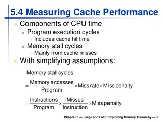
Memory and overall performance How do cache hits and misses affect overall system performance? --Assuming a hit time of one CPU clock cycle, program execution will continue normally on a cache hit. -- For cache misses, we ll assume the CPU must stall to wait for a load from main memory. The total number of stall cycles depends on the number of cache misses and the miss penalty. Memory stall cycles = Memory accesses x miss rate x miss penalty To include stalls due to cache misses in CPU performance equations: CPU time = (CPU execution cycles + Memory stall cycles) x Cycle time
Example Assume that 33% of the instructions in a program are data accesses. The cache hit ratio is 97% and the hit time is one cycle, but the miss penalty is 20 cycles. Memory stall cycles = Memory accesses x Miss rate x Miss penalty = 0.33 I x 0.03 x 20 cycles = 0.2 I cycles Processor performance traditionally outpaces memory performance, so the memory system is often the system bottleneck. In this example, with a base CPI of 1, the CPU time is: CPU time = (I + 0.2 I) x Cycle time What if we could double the CPU performance so the CPI becomes 0.5, but memory performance remained the same? CPU time = (0.5 I + 0.2 I) x Cycle time The overall CPU time improves by just 1.2/0.7 = 1.7 times!
Basic main memory design There are some ways the main memory can be organized to reduce miss penalties and help with caching. For examples assume the following three steps are taken when a cache needs to load data from the main memory. 1. It takes 1 cycle to send an address to the RAM. 2. There is a 15-cycle latency for each RAM access. 3. It takes 1 cycle to return data from the RAM. In the setup shown here, the buses from the CPU to the cache and from the cache to RAM are all one word wide. If the cache has one-word blocks, then filling a block from RAM (i.e., the miss penalty) would take 17 cycles. CPU Cache Main Memory 1 + 15 + 1 = 17 clock cycles The cache controller has to send the desired address to the RAM, wait and receive the data.
Miss penalties for larger cache blocks If the cache has four-word blocks, then loading a single block would need four individual main memory accesses, and a miss penalty of 68 cycles. CPU Cache Main Memory
A wider memory A simple way to decrease the miss penalty is to widen memory and its interface to cache for multiple words from RAM. If four words are read from the memory at once, a four- word cache load would need just 17 cycles. 1 + 15 + 1 = 17 cycles The disadvantage is the cost of the wider buses each additional bit of memory width requires another connection to the cache. CPU Cache Main Memory
An interleaved memory Another approach is to interleave the memory, or split it into banks that can be accessed individually. The main benefit is overlapping the latencies of accessing each word. For example, if our main memory has four banks, each one word wide, then we could load four words into a cache block in just 20 cycles. CPU Cache Main Memory 1 + 15 + (4 x 1) = 20 cycles Bank 0 Bank 1 Bank 2 Bank 3 Our buses are still one word wide here, so four cycles are needed to transfer data to the caches.
Example Each memory bank has a 15-cycle latency, and it takes another cycle (shown in blue) to return data from the memory. The same basic idea as pipelining. As soon as we request data from one memory bank, we can go ahead and request data from another bank as well. Each individual load takes 17 clock cycles, but four overlapped loads require just 20 cycles. Clock cycles Load word 1 Load word 2 Load word 3 Load word 4 15 cycles
End of Lectures End of Lectures 35


