Enhancing NAND Flash Memory Lifetime Through Data Retention Optimization
Characterization, optimization, and recovery methods are explored to extend the lifespan of MLC NAND flash memory. Challenges such as high raw bit error rates and charge leakage leading to retention loss are addressed. Techniques like ECC and threshold voltage adjustment are employed to improve memory endurance and reduce errors over time.

Uploaded on Aug 14, 2024 | 0 Views
Download Presentation

Please find below an Image/Link to download the presentation.
The content on the website is provided AS IS for your information and personal use only. It may not be sold, licensed, or shared on other websites without obtaining consent from the author.If you encounter any issues during the download, it is possible that the publisher has removed the file from their server.
You are allowed to download the files provided on this website for personal or commercial use, subject to the condition that they are used lawfully. All files are the property of their respective owners.
The content on the website is provided AS IS for your information and personal use only. It may not be sold, licensed, or shared on other websites without obtaining consent from the author.
E N D
Presentation Transcript
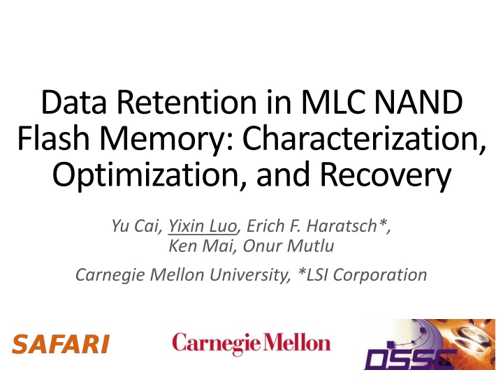
Data Retention in MLC NAND Flash Memory: Characterization, Optimization, and Recovery Yu Cai, Yixin Luo, Erich F. Haratsch*, Ken Mai, Onur Mutlu Carnegie Mellon University, *LSI Corporation 1
You Probably Know Many use cases: + High performance, low energy consumption 2
NAND Flash Memory Challenges Requires erase before program (write) High raw bit error rate Controller Raw Flash Memory Chips Flash CPU ECC Controller 3
Limited Flash Memory Lifetime Goal: Extend flash memory lifetime at low cost Raw bit error rate (RBER) P/E Cycle Lifetime ECC-correctable RBER ~2000 ~3000 Program/Erase (P/E) Cycles (or Writes Per Cell) 4
Retention Loss Charge leakage over time 0 0 1 Retention error Flash cell One dominant source of flash memory errors [DATE 12, ICCD 12] 5
Before I show you how we extend flash lifetime NAND Flash 101 6
Threshold Voltage (Vth) Flash cell Flash cell 0 1 Normalized Vth 7
Threshold Voltage (Vth) Distribution Probability Density Function (PDF) 0 1 Normalized Vth 8
Read Reference Voltage (Vref) PDF Vref 0 1 Normalized Vth 9
Multi-Level Cell (MLC) ER-P1 Vref P1-P2 Vref P2-P3 Vref PDF Erased (11) P1 (10) P2 (00) P3 (01) Normalized Vth 10
Threshold Voltage Reduces Over Time Before retention loss: After some retention loss: PDF P1 (10) P2 (00) P3 (01) Normalized Vth 11
Fixed Read Reference Voltage Becomes Suboptimal Before retention loss: After some retention loss: P2-P3 Vref P1-P2 Vref PDF P1 (10) P2 (00) P3 (01) Normalized Vth Normalized Vth Raw bit errors 12
Optimal Read Reference Voltage (OPT) After some retention loss: P1-P2 OPT P2-P3 OPT P2-P3 Vref P1-P2 Vref PDF P1 (10) P2 (00) P3 (01) Normalized Vth Minimal raw bit errors 13
Goal 1: Design a low-cost mechanism that dynamically finds the optimal read reference voltage 14
Retention Failure After some retention loss: After significant retention loss: P2-P3 Vref P1-P2 Vref PDF P1 (10) P2 (00) P3 (01) Normalized Vth Correctable errors Uncorrectable errors 15
Goal 1: Design a low-cost mechanism that dynamically finds the optimal read reference voltage Goal 2: Design an offline mechanism to recover data after detecting uncorrectable errors 16
To understand the effects of retention loss: - Characterize retention loss using real chips 17
To understand the effects of retention loss: - Characterize retention loss using real chips Goal 1: Design a low-cost mechanism that dynamically finds the optimal read reference voltage Goal 2: Design an offline mechanism to recover data after detecting uncorrectable errors 18
Characterization Methodology FPGA-based flash memory testing platform [Cai+,FCCM 11] 19
Characterization Methodology FPGA-based flash memory testing platform Real Real 20- to 24-nm MLC NAND flash chips 0- to 40-day worth of retention loss Room temperature (20 C) 0 to 50k P/E Cycles 20
Characterize the effects of retention loss 1. Threshold Voltage Distribution 2. Optimal Read Reference Voltage 3. RBER and P/E Cycle Lifetime 21
1. Threshold Voltage (Vth) Distribution PDF P1 P2 P3 Normalized Vth 22
1. Threshold Voltage (Vth) Distribution 0-day 0-day 40-day 40-day P1 P2 P3 Finding: Cell s threshold voltage decreases over time 23
2. Optimal Read Reference Voltage (OPT) 40-day OPT 0-day OPT 40-day OPT 0-day OPT P1 P2 P3 Finding: OPT decreases over time 24
3. RBER and P/E Cycle Lifetime RBER P/E Cycles 25
3. RBER and P/E Cycle Lifetime Vref closer to actual OPT Reading data with 7-day worth of retention loss. Extended Nominal Lifetime Lifetime Actual OPT ECC-correctable RBER Finding: Using actual OPT achieves the longest lifetime 26
Characterization Summary Due to retention loss retention loss Cell s threshold voltage Cell s threshold voltage (Vth) decreases over time Optimal read reference voltage Optimal read reference voltage (OPT) decreases over time Using the actual OPT actual OPT for reading Achieves the longest lifetime lifetime 27
To understand the effects of retention loss: - Characterize retention loss using real chips Goal 1: Design a low-cost mechanism that dynamically finds the optimal read reference voltage Goal 2: Design an offline mechanism to recover data after detecting uncorrectable errors 28
Nave Solution: Sweeping Vref Key idea: Read the data multiple times with different read reference voltages until the raw bit errors are correctable by ECC Finds the optimal read reference voltage Requires many read-retries higher read latency 29
Comparison of Flash Read Techniques Flash Read Techniques Lifetime (P/E Cycle) Performance (Read Latency) Fixed Vref Sweeping Vref Our Goal 30
Observations 1. The optimal read reference voltage gradually decreases over time Key idea: Record the old OPT as a prediction (Vpred) of the actual OPT Benefit: Close to actual OPT Fewer read retries 2. The amount of retention loss is similar across pages within a flash block Key idea: Record only one Vpred for each block Benefit: Small storage overhead (768KB out of 512GB) 31
Retention Optimized Reading (ROR) Components: 1. Online pre-optimization algorithm Periodically records a Vpred for each block 2. Improved read-retry technique Utilizes the recorded Vpred to minimize read-retry count 32
1. Online Pre-Optimization Algorithm Triggered periodically (e.g., per day) Find and record an OPT as per-block Vpred Performed in background Small storage overhead New Vpred Old Vpred PDF Normalized Vth 33
2. Improved Read-Retry Technique Performed as normal read Vpred already close to actual OPT Decrease Vref if Vpred fails, and retry PDF OPT Vpred Normalized Vth Very close 34
Retention Optimized Reading: Summary Flash Read Techniques Lifetime (P/E Cycle) 64% 64% Performance (Read Latency) _____ Ext. Life: 70.4% Fixed Vref Sweeping Vref Nom. Life: 2.4% ROR 35
To understand the effects of retention loss: - Characterize retention loss using real chips Goal 1: Design a low-cost mechanism that dynamically finds the optimal read reference voltage Goal 2: Design an offline mechanism to recover data after detecting uncorrectable errors 36
Retention Failure After some retention loss: After significant retention loss: P2-P3 Vref P1-P2 Vref PDF P1 (10) P2 (00) P3 (01) Normalized Vth Correctable errors Uncorrectable errors 37
Leakage Speed Variation PDF low-leaking cell S S ast-leaking cell F F Normalized Vth 38
Initially, Right After Programming PDF P2 P3 S S F F F F S S Normalized Vth 39
After Some Retention Loss Fast-leaking cells have lower Vth PDF Slow-leaking cells have higher Vth P2 P3 S S F F F F F F F F S S Normalized Vth 40
Eventually: Retention Failure PDF OPT P2 P3 S S F F F F S S Normalized Vth 41
Retention Failure Recovery (RFR) Key idea: Guess original state of the cell from its leakage speed property Three steps 1. Identify risky cells 2. Identify fast-/slow-leaking cells 3. Guess original states 42
1. Identify Risky Cells OPT+ OPT + S = P2 Risky cells PDF OPT + F = Key Formula P3 S F F S Normalized Vth 43
2. Identifying Fast- vs. Slow-Leaking Cells OPT+ OPT + S = P2 Risky cells PDF OPT + F = Key Formula P3 ? ? ? ? ? ? Normalized Vth 44
2. Identifying Fast- vs. Slow-Leaking Cells OPT+ OPT + S = P2 Risky cells PDF OPT + F = Key Formula P3 ? S ? ? F ? ? F ? S Normalized Vth 45
3. Guess Original States + S = P2 Risky cells PDF + F = Key Formula P3 S F F S Normalized Vth 46
RFR Evaluation Expect to eliminate 50% of raw bit errors ECC can correct remaining errors Program with random data 28 days Detect failure, backup data 12 addt l. days Recover data 47
To understand the effects of retention loss: - Characterize retention loss using real chips Goal 1: Design a low-cost mechanism that dynamically finds the optimal read reference voltage Goal 2: Design an offline mechanism to recover data after detecting uncorrectable errors 48
Conclusion Problem: Retention loss reduces flash lifetime Overall Goal: Extend flash lifetime at low cost Flash Characterization: Developed an understanding of the effects of retention loss in real chips Retention Optimized Reading: A low-cost mechanism that dynamically finds the optimal read reference voltage 64% lifetime , 70.4% read latency Retention Failure Recovery: An offline mechanism that recovers data after detecting uncorrectable errors Raw bit error rate 50% , reduces data loss 49
Data Retention in MLC NAND Flash Memory: Characterization, Optimization, and Recovery Yu Cai, Yixin Luo, Erich F. Haratsch*, Ken Mai, Onur Mutlu Carnegie Mellon University, *LSI Corporation 50


")
 Distribution")
")
")


")


 Distribution")
 Distribution")
")


")


")