Energy Level Formation in Semiconductor Materials

F
i
g
u
r
e
3
E
n
e
r
g
y
l
e
v
e
l
s
:
(
a
)
d
i
s
c
r
e
t
e
l
e
v
e
l
s
i
n
i
s
o
l
a
t
e
d
a
t
o
m
i
c
s
t
r
u
c
t
u
r
e
s
;
(
b
)
c
o
n
d
u
c
t
i
o
n
a
n
d
v
a
l
e
n
c
e
b
a
n
d
s
o
f
a
n
i
n
s
u
l
a
t
o
r
,
s
e
m
i
c
o
n
d
u
c
t
o
r
,
a
n
d
c
o
n
d
u
c
t
o
r
.

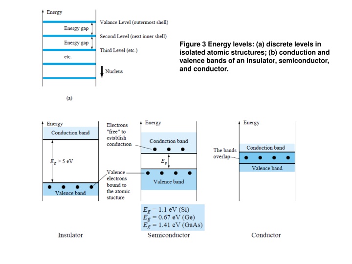
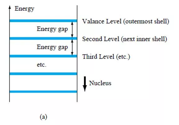
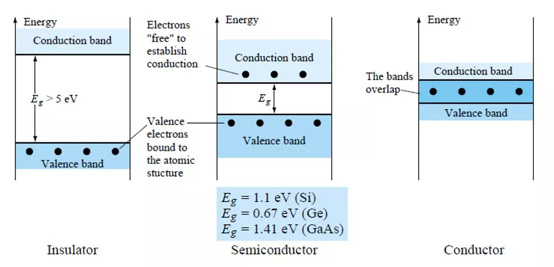
The net result is an expansion of the discrete levels of possible energy states
for the valence electrons to that of bands as shown in Fig. 3b. Note that there are
boundary levels and maximum energy states in which any electron in the atomic
lattice can find itself, and there remains a
forbidden region between the valence
band and the ionization level.
4
.
E
X
T
R
I
N
S
I
C
M
A
T
E
R
I
A
L
S
—
n
-
A
N
D
p
-
T
Y
P
E
A
s
e
m
i
c
o
n
d
u
c
t
o
r
m
a
t
e
r
i
a
l
t
h
a
t
h
a
s
b
e
e
n
s
u
b
j
e
c
t
e
d
t
o
t
h
e
d
o
p
i
n
g
p
r
o
c
e
s
s
i
s
c
a
l
l
e
d
a
n
e
x
t
r
i
n
s
i
c
m
a
t
e
r
i
a
l
.
T
h
e
r
e
a
r
e
t
w
o
e
x
t
r
i
n
s
i
c
m
a
t
e
r
i
a
l
s
o
f
i
m
m
e
a
s
u
r
a
b
l
e
i
m
p
o
r
t
a
n
c
e
t
o
s
e
m
i
c
o
n
d
u
c
t
o
r
device fabrication:
n-type and p-type. Each will be described in some detail in the
following paragraphs.
4
.
1
n
-
T
y
p
e
M
a
t
e
r
i
a
l
Both the
n- and p-type materials are formed by adding a predetermined
number of
impurity atoms into a germanium or silicon base. The
n-type is
created by introducing
those impurity elements that have
five valence
electrons (pentavalent), such as antimony, arsenic, and phosphorus. The
effect of such impurity elements is indicated in
Fig. 4 (using antimony as the
impurity in a silicon base). Note that the four covalent bonds are still present.
There is, however, an additional fifth electron due to the impurity atom, which
is
unassociated with any particular covalent bond.
F
i
g
u
r
e
4
A
n
t
i
m
o
n
y
i
m
p
u
r
i
t
y
i
n
n
-
t
y
p
e
m
a
t
e
r
i
a
l
D
i
f
f
u
s
e
d
i
m
p
u
r
i
t
i
e
s
w
i
t
h
f
i
v
e
v
a
l
e
n
c
e
e
l
e
c
t
r
o
n
s
a
r
e
c
a
l
l
e
d
d
o
n
o
r
a
t
o
m
s
.
T
h
e
e
f
f
e
c
t
o
f
t
h
i
s
d
o
p
i
n
g
p
r
o
c
e
s
s
o
n
t
h
e
r
e
l
a
t
i
v
e
c
o
n
d
u
c
t
i
v
i
t
y
c
a
n
b
e
s
t
b
e
d
e
s
c
r
i
b
e
d
t
h
r
o
u
g
h
t
h
e
u
s
e
o
f
t
h
e
e
n
e
r
g
y
-
b
a
n
d
d
i
a
g
r
a
m
o
f
F
i
g
.
5
.
N
o
t
e
t
h
a
t
a
d
i
s
c
r
e
t
e
e
n
e
r
g
y
l
e
v
e
l
(
c
a
l
l
e
d
t
h
e
d
o
n
o
r
l
e
v
e
l
)
a
p
p
e
a
r
s
i
n
t
h
e
f
o
r
b
i
d
d
e
n
b
a
n
d
w
i
t
h
a
n
E
g
s
i
g
n
i
f
i
c
a
n
t
l
y
l
e
s
s
t
h
a
n
t
h
a
t
o
f
t
h
e
i
n
t
r
i
n
s
i
c
m
a
t
e
r
i
a
l
.
F
i
g
u
r
e
5
E
f
f
e
c
t
o
f
d
o
n
o
r
i
m
p
u
r
i
t
i
e
s
o
n
t
h
e
e
n
e
r
g
y
b
a
n
d
s
t
r
u
c
t
u
r
e
.
4
.
2
p
-
T
y
p
e
M
a
t
e
r
i
a
l
The
p-type material is formed by doping a pure germanium or silicon crystal
with
impurity atoms having
three valence electrons. The elements most
frequently used for
this purpose are
boron, gallium, and indium. The effect of
one of these elements,
boron, on a base of silicon is indicated in Fig. 6
Energy levels in isolated atomic structures form discrete levels which expand to bands in insulators, semiconductors, and conductors. Extrinsic materials like n-type and p-type are created by doping semiconductors with impurity atoms to alter conductivity. The n-type material involves adding pentavalent impurity atoms like antimony, while the p-type material uses trivalent impurity atoms such as boron. These impurity atoms create additional energy levels within the bands, affecting the conductivity of the semiconductor material.

Download Presentation

Please find below an Image/Link to download the presentation.
The content on the website is provided AS IS for your information and personal use only. It may not be sold, licensed, or shared on other websites without obtaining consent from the author.If you encounter any issues during the download, it is possible that the publisher has removed the file from their server.
You are allowed to download the files provided on this website for personal or commercial use, subject to the condition that they are used lawfully. All files are the property of their respective owners.
The content on the website is provided AS IS for your information and personal use only. It may not be sold, licensed, or shared on other websites without obtaining consent from the author.
E N D
Presentation Transcript
Figure 3 Energy levels: (a) discrete levels in isolated atomic structures; (b) conduction and valence bands of an insulator, semiconductor, and conductor.
The net result is an expansion of the discrete levels of possible energy states for the valence electrons to that of bands as shown in Fig. 3b. Note that there are boundary levels and maximum energy states in which any electron in the atomic lattice can find itself, and there remains a forbidden region between the valence band and the ionization level. 4. EXTRINSIC MATERIALS n- AND p-TYPE A semiconductor material that has been subjected to the doping process is called an extrinsic material. There are two extrinsic materials of immeasurable importance to semiconductor device fabrication: n-type and p-type. Each will be described in some detail in the following paragraphs. 4.1 n-Type Material Both the n- and p-type materials are formed by adding a predetermined number of impurity atoms into a germanium or silicon base. The n-type is created by introducing those impurity elements that have five valence electrons (pentavalent), such as antimony, arsenic, and phosphorus. The effect of such impurity elements is indicated in Fig. 4 (using antimony as the impurity in a silicon base). Note that the four covalent bonds are still present. There is, however, an additional fifth electron due to the impurity atom, which is unassociated with any particular covalent bond.
Figure 4 Antimony impurity in n-type material Diffused impurities with five valence electrons are called donor atoms. The effect of this doping process on the relative conductivity can best be described through the use of the energy-band diagram of Fig. 5. Note that a discrete energy level (called the donor level) appears in the forbidden band with an Eg significantly less than that of the intrinsic material.
Figure 5 Effect of donor impurities on the energy band structure. 4.2 p-Type Material The p-type material is formed by doping a pure germanium or silicon crystal with impurity atoms having three valence electrons. The elements most frequently used for this purpose are boron, gallium, and indium. The effect of one of these elements,boron, on a base of silicon is indicated in Fig. 6
 discrete levels in")