Digital Logic Design with Alex Bronstein


D
i
g
i
t
a
l
L
o
g
i
c
D
e
s
i
g
n
234262
Alex Bronstein


C
o
m
p
u
t
e
r
s
A
r
o
u
n
d
U
s


C
o
u
r
s
e
G
o
a
l
s
Learn how to design logic systems
Learn the design of a simple CPU (MIPS)
Stop worrying and learn to love digital systems
S
h
o
r
t
b
i
o
I
n
t
h
e
A
c
a
d
e
m
i
a
:
B.Sc. and M.Sc. in EE, Technion (1998-2005)
Ph.D. in CS, Technion (2005-2007)
Prof., EE@Tel Aviv University (2010-2016)
Prof., CS@Technion (from 2016)
Research interests: computer vision, machine learning, computational
geometry, imaging and image processing
I
n
t
h
e
I
n
d
u
s
t
r
y
:
Cofounder and VP Technology, Novafora Inc. (2006-2009)
Cofounder, Invision Ltd. (2009-2012)
Research Scientist & Principal Engineer, Intel Corporation (from 2012)
Cofounder and Chief Scientist, Videocites Ltd. (from 2014)
C
o
u
r
s
e
S
t
a
f
f
A
l
e
x
B
r
o
n
s
t
e
i
n
(
l
e
c
t
u
r
e
r
i
n
c
h
a
r
g
e
)
Taub 719
bron@cs.technion.ac.il
C
h
a
i
m
B
a
s
k
i
n
(
l
e
c
t
u
r
e
r
)
Taub 700
chaimbaskin@cs.technio.ac.il
N
o
a
m
Y
e
f
f
e
t
(
T
A
i
n
c
h
a
r
g
e
)
T
a
u
b
3
2
7
s
n
y
e
f
e
t
@
c
s
.
t
e
c
h
n
i
o
n
.
a
c
.
i
l
T
o
m
m
y
B
o
j
a
n
(
T
A
)
T
a
u
b
7
1
7
t
o
m
m
y
.
B
o
j
a
n
@
i
n
t
e
l
.
c
o
m
A
l
o
n
G
u
e
t
a
(
T
A
)
Taub TBD alon.gueta@campus.technion.ac.il
A
v
i
r
a
m
I
m
b
e
r
(
T
A
)
T
a
u
b
2
1
3
a
v
i
r
a
m
.
i
m
b
e
r
@
c
a
m
p
u
s
.
t
e
c
h
n
i
o
n
.
a
c
.
i
l
B
a
h
j
a
t
K
a
w
a
r
(
T
A
)
Taub 213 bahjat.kawar@campus.technion.ac.il
M
o
s
h
e
L
i
e
c
h
t
e
n
s
t
e
i
n
(
T
A
)
Taub 437 smosesli@cs.technion.ac.il
C
o
u
r
s
e
F
o
r
m
a
l
i
t
i
e
s
G
r
a
d
e
:
25% home assignments
75% final exam
A
s
s
i
g
n
m
e
n
t
s
:
2 “dry” exercises (2.5%)
2
“
w
e
t
”
V
e
r
i
l
o
g
c
o
d
i
n
g
e
x
e
r
c
i
s
e
s
(
1
0
%
e
a
c
h
)
Passing grade (>54) mandatory in each of the “wet” exercises
H
a
r
d
w
a
r
e
H
a
r
d
w
a
r
e
H
a
r
d
w
a
r
e
H
a
r
d
w
a
r
e
D
e
s
i
g
n
F
l
o
w
(
A
S
I
C
)
Design specs
Architecture
RTL design
Functional verification
Logic synthesis
Floor planning
Placement & routing
Physical verification
Tapeout
Mask tooling
Fabrication
Packaging
F
r
o
n
t
e
n
d
B
a
c
k
e
n
d
F
o
u
n
d
r
y
Technology
library
Static timing analysis
H
a
r
d
w
a
r
e
D
e
s
i
g
n
F
l
o
w
(
F
P
G
A
)
Design specs
Architecture
RTL design
Functional verification
Logic synthesis
Placement & routing
S
o
f
t
w
a
r
e
D
e
s
i
g
n
F
l
o
w
Design specs
Architecture
High-level code
Compilation
S
o
f
t
w
a
r
e
v
s
.
H
a
r
d
w
a
r
e
S
o
f
t
w
a
r
e
H
a
r
d
w
a
r
e
Design cost
Low
High
Design cycle
Fast
Slow
Language
High-level languages
HDL
(Java, C#, C++, C)
(Verilog, VHDL)
Code undergoes
Compilation
Synthesis
Parallelism
Usually sequential
Inherently parallel
(SIMD, threading, IPC)
Target platforms
CPU
FPGA or ASIC
(x86,ARM,GPU,DSP)
(lots of processes)
G
o
o
d
E
n
g
i
n
e
e
r
i
n
g
P
r
a
c
t
i
c
e
s
M
o
d
u
l
a
r
i
t
y
Design basic building blocks (modules)
Connect modules together to form another module
A module can be replaced by a new version without affecting the rest
of the system
S
t
a
n
d
a
r
d
i
z
a
t
i
o
n
Using a library with a small amount of standard modules
Clearly defined functionality and interfaces
Don’t reinvent the wheel
A
b
s
t
r
a
c
t
i
o
n
Decomposition of design process into a hierarchy of levels
Hide unnecessary lower-level details
A
b
s
t
r
a
c
t
i
o
n
Simplifies design and understanding of complex systems
A higher level of abstraction is based on the level beneath
A higher level of abstraction hides details of lower levels
Always try to solve problems at the highest possible level of abstraction
Example of abstraction hierarchy:
High-level language
Machine language
Register-transfer level (RTL)
Gate level, analog electronics
Physics
A
b
s
t
r
a
c
t
i
o
n
v
s
.
I
m
p
l
e
m
e
n
t
a
t
i
o
n
A
b
s
t
r
a
c
t
i
o
n
:
l
o
w
l
e
v
e
l
h
i
g
h
e
r
l
e
v
e
l
I
m
p
l
e
m
e
n
t
a
t
i
o
n
:
h
i
g
h
l
e
v
e
l
l
o
w
e
r
l
e
v
e
l
Abstraction requires adhering to a certain set of rules to be valid
High-level language:
variable
Register-transfer level:
register
Gate level:
NAND gates
Physics:
p-type and n-type MOSFETs
A
b
s
t
r
a
c
t
i
o
n
o
f
D
i
g
i
t
a
l
S
y
s
t
e
m
s
P
h
y
s
i
c
a
l
L
o
g
i
c
a
l
Input:
V
in
> V
IH
1
Output:
V
out
> V
OH
1
Input:
V
in
< V
IL
0
Output:
V
out
< V
OL
0
V
IL
< V < V
IH
undefined
N
o
i
s
e
m
a
r
g
i
n
s
i
n
c
r
e
a
s
e
r
o
b
u
s
t
n
e
s
s
t
o
n
o
i
s
e
a
d
d
e
d
t
o
s
i
g
n
a
l
p
a
s
s
i
n
g
f
r
o
m
t
h
e
o
u
t
p
u
t
o
f
o
n
e
c
o
m
p
o
n
e
n
t
t
o
t
h
e
i
n
p
u
t
o
f
a
n
o
t
h
e
r
Allows modularity!
V
IH
V
OH
V
OL
V
IL
noise
margin
noise
margin
V
T
i
m
i
n
g
C
o
n
t
a
m
i
n
a
t
i
o
n
d
e
l
a
y
(
t
C
D
)
–
m
i
n
i
m
u
m
t
i
m
e
f
o
l
l
o
w
i
n
g
i
n
p
u
t
c
h
a
n
g
e
d
u
r
i
n
g
w
h
i
c
h
v
a
l
i
d
i
t
y
o
f
p
r
e
v
i
o
u
s
o
u
t
p
u
t
i
s
g
u
a
r
a
n
t
e
e
d
P
r
o
p
a
g
a
t
i
o
n
d
e
l
a
y
(
t
P
D
)
–
m
a
x
i
m
u
m
t
i
m
e
f
o
l
l
o
w
i
n
g
i
n
p
u
t
c
h
a
n
g
e
a
f
t
e
r
w
h
i
c
h
t
h
e
v
a
l
i
d
i
t
y
o
f
n
e
w
o
u
t
p
u
t
i
s
g
u
a
r
a
n
t
e
e
d
V
IH
V
IL
V
in
t
V
OH
V
OL
V
out
t
t
CD
t
CD
t
PD
t
PD
C
o
m
b
i
n
a
t
i
o
n
a
l
L
o
g
i
c
(
C
L
)
O
u
t
p
u
t
=
B
o
o
l
e
a
n
f
u
n
c
t
i
o
n
o
f
t
h
e
i
n
p
u
t
B
u
i
l
d
i
n
g
b
l
o
c
k
s
:
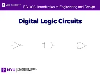
Logic gates
Wires
Combinational logic sub-systems
B
u
i
l
d
i
n
g
r
u
l
e
s
:
No feedback
No floating wires (except inputs and outputs)
N
u
m
b
e
r
o
f
i
n
p
u
t
s
e
a
c
h
o
u
t
p
u
t
d
r
i
v
e
s
d
o
e
s
n
o
t
e
x
c
e
e
d
f
a
n
o
u
t
l
i
m
i
t
a
t
i
o
n
s
S
t
a
t
i
c
T
i
m
i
n
g
I
f
i
n
p
u
t
s
t
o
C
L
s
y
s
t
e
m
a
r
e
v
a
l
i
d
a
n
d
s
t
a
b
l
e
,
a
f
t
e
r
s
e
t
t
l
i
n
g
t
i
m
e
,
o
u
t
p
u
t
s
a
r
e
a
l
s
o
v
a
l
i
d
a
n
d
s
t
a
b
l
e
Allows resilience to inaccurate analog components
Prevents noise accumulation during signal propagation
A
l
l
o
w
s
c
h
e
a
p
m
a
s
s
p
r
o
d
u
c
t
i
o
n
o
f
c
o
m
p
o
n
e
n
t
s
OLD
NEW, Stable
OLD
NEW, Stable
OLD
NEW, Stable
INPUT
OUTPUT
1
OUTPUT
2
S
t
a
t
i
c
T
i
m
i
n
g
E
x
a
m
p
l
e
:
I
n
v
e
r
t
e
r
(
N
O
T
g
a
t
e
)
V
in
< V
IL
V
out
> V
OH
V
in
> V
IH
V
out
< V
OL
V
OH
V
OL
V
out
V
IL
V
IH
V
in
Actual components have different
analog characteristics due to
Fabrication tolerances
Temperature changes
Supply voltage fluctuations
S
t
a
t
i
c
T
i
m
i
n
g
C
o
n
t
a
m
i
n
a
t
i
o
n
d
e
l
a
y
(
t
C
D
)
–
m
i
n
i
m
u
m
t
i
m
e
f
o
l
l
o
w
i
n
g
i
n
p
u
t
c
h
a
n
g
e
d
u
r
i
n
g
w
h
i
c
h
v
a
l
i
d
i
t
y
o
f
a
l
l
p
r
e
v
i
o
u
s
o
u
t
p
u
t
s
i
s
g
u
a
r
a
n
t
e
e
d
Components in parallel:
min of t
CD
Components in series:
sum of t
CD
P
r
o
p
a
g
a
t
i
o
n
d
e
l
a
y
(
t
P
D
)
–
m
a
x
i
m
u
m
t
i
m
e
f
o
l
l
o
w
i
n
g
i
n
p
u
t
c
h
a
n
g
e
a
f
t
e
r
w
h
i
c
h
t
h
e
v
a
l
i
d
i
t
y
o
f
a
l
l
n
e
w
o
u
t
p
u
t
i
s
g
u
a
r
a
n
t
e
e
d
Components in parallel:
max of t
PD
Components in series:
sum of t
PD
S
y
n
c
h
r
o
n
o
u
s
S
t
a
t
i
c
M
e
m
o
r
y
P
o
s
i
t
i
v
e
e
d
g
e
-
t
r
i
g
g
e
r
e
d
D
f
l
i
p
-
f
l
o
p
(
D
F
F
)
L
o
g
i
c
a
l
c
h
a
r
a
c
t
e
r
i
s
t
i
c
:
Output Q assumes the value of D after CLK rise
T
i
m
i
n
g
c
h
a
r
a
c
t
e
r
i
s
t
i
c
:
I
f
i
n
p
u
t
i
s
h
e
l
d
c
o
n
s
t
a
n
t
t
S
U
b
e
f
o
r
e
a
n
d
t
H
a
f
t
e
r
c
l
o
c
k
r
i
s
e
t
h
e
n
old output will stay valid at least t
cCQ
and new output will become valid
at most t
pCQ
after clock rise
NEW
OLD
NEW
CLK
D
Q
t
SU
t
H
t
cCQ
t
pCQ
S
y
n
c
h
r
o
n
o
u
s
S
t
a
t
i
c
M
e
m
o
r
y
S
y
n
c
h
r
o
n
o
u
s
S
e
q
u
e
n
t
i
a
l
L
o
g
i
c
S
t
a
t
e
m
a
c
h
i
n
e
s
B
u
i
l
d
i
n
g
b
l
o
c
k
s
:
Combinational logic modules
Clocked memory modules
Wires
B
u
i
l
d
i
n
g
r
u
l
e
s
:
No CL loops unless through at least one memory module
Clock period long enough to satisfy timing requirements
All inputs remain stable enough time to satisfy timing requirements
F
i
n
i
t
e
S
t
a
t
e
M
a
c
h
i
n
e
s
(
F
S
M
)
C
L
U
1
U
n
…
Y
1
Y
m
…
X
1
X
k
…
X’
1
X’
k
…
M
E
M
O
R
Y
I
N
P
U
T
S
O
U
T
P
U
T
S
P
R
E
S
E
N
T
S
T
A
T
E
N
E
X
T
S
T
A
T
E
A finite set of states X
{0,…,K-1}k bits represent 2
k
states
n-bit input U
m-bit output Y
S
t
a
t
e
u
p
d
a
t
e
f
u
n
c
t
i
o
n
:
X[t+1] =
(X[t],U[t])
O
u
t
p
u
t
f
u
n
c
t
i
o
n
:
Mealy FSM:
Y[t] =
(X[t],U[t])
Moore FSM:
Y[t] =
(X[t])
F
S
M
T
i
m
i
n
g
C
L
U
Y
X
X’
D
F
F
s
CLK
t
pCQ
t
PD
t
SU
C
l
o
c
k
p
e
r
i
o
d
T
>
t
p
C
Q
+
t
P
D
+
t
S
U
F
S
M
T
i
m
i
n
g
C
L
U
Y
X
X’
D
F
F
s
CLK
t
PD
t
SU
C
l
o
c
k
p
e
r
i
o
d
T
>
t
p
C
Q
+
t
P
D
+
t
S
U
I
n
p
u
t
s
e
t
u
p
t
i
m
e
t
S
U
(
U
)
>
t
P
D
(
C
L
)
+
t
S
U
F
S
M
T
i
m
i
n
g
C
L
U
Y
X
X’
D
F
F
s
CLK
C
l
o
c
k
p
e
r
i
o
d
T
>
t
p
C
Q
+
t
P
D
+
t
S
U
I
n
p
u
t
s
e
t
u
p
t
i
m
e
t
S
U
(
U
)
>
t
P
D
(
C
L
)
+
t
S
U
I
n
p
u
t
h
o
l
d
t
i
m
e
t
H
(
U
)
>
t
H
(
D
F
F
)
-
t
C
D
(
C
L
)
A
d
d
i
t
i
o
n
a
l
T
i
m
i
n
g
C
o
n
s
i
d
e
r
a
t
i
o
n
s
C
l
o
c
k
s
k
e
w
:
c
l
o
c
k
s
i
g
n
a
l
a
r
r
i
v
e
s
with different delay to different
memories
C
l
o
c
k
j
i
t
t
e
r
:
c
l
o
c
k
i
s
n
o
t
e
x
a
c
t
l
y
p
e
r
i
o
d
i
c
A
s
y
n
c
h
r
o
n
o
u
s
i
n
p
u
t
s
m
a
y
v
i
o
l
a
t
e
h
o
l
d
r
e
q
u
i
r
e
m
e
n
t
a
n
d
c
a
u
s
e
m
e
t
a
s
t
a
b
i
l
i
t
y
L
a
t
e
n
c
y
a
n
d
T
h
r
o
u
g
h
p
u
t
L
a
t
e
n
c
y
:
a
m
o
u
n
t
o
f
t
i
m
e
p
a
s
s
i
n
g
b
e
t
w
e
e
n
t
h
e
b
e
g
i
n
n
i
n
g
o
f
a
c
a
l
c
u
l
a
t
i
o
n
a
n
d
i
t
s
e
n
d
(
i
n
p
u
t
-
t
o
-
o
u
t
p
u
t
d
e
l
a
y
)
T
h
r
o
u
g
h
p
u
t
:
r
a
t
e
a
t
w
h
i
c
h
c
a
l
c
u
l
a
t
i
o
n
s
a
r
e
p
e
r
f
o
r
m
e
d
(
=
c
a
l
c
u
l
a
t
i
o
n
s
p
e
r
u
n
i
t
o
f
t
i
m
e
)
L
a
t
e
n
c
y
a
n
d
T
h
r
o
u
g
h
p
u
t
Example: sum of N numbers
MEM
S
e
q
u
e
n
t
i
a
l
i
m
p
l
e
m
e
n
t
a
t
i
o
n
Latency
= N×t
0
Throughput
= 1/(N×t
0
)
C
o
m
b
i
n
a
t
i
o
n
a
l
i
m
p
l
e
m
e
n
t
a
t
i
o
n
Latency
= log
2
N×t
0
Throughput
= 1/(log
2
N×t
0
)
In this course, delve into digital logic design concepts with Alex Bronstein. Explore the fundamentals of designing logic systems and learn the intricacies of a simple CPU design. Gain insights into the world of digital systems and their applications. The course covers a range of topics from hardware design to formalities such as assignments and examinations. Meet the course staff responsible for guiding you through this educational journey. Discover the hardware design flow, including ASIC and FPGA technologies, and various stages in the design process. Embrace the opportunity to enhance your knowledge in digital logic design under the mentorship of experienced professionals.

Download Presentation

Please find below an Image/Link to download the presentation.
The content on the website is provided AS IS for your information and personal use only. It may not be sold, licensed, or shared on other websites without obtaining consent from the author.If you encounter any issues during the download, it is possible that the publisher has removed the file from their server.
You are allowed to download the files provided on this website for personal or commercial use, subject to the condition that they are used lawfully. All files are the property of their respective owners.
The content on the website is provided AS IS for your information and personal use only. It may not be sold, licensed, or shared on other websites without obtaining consent from the author.
E N D
Presentation Transcript
1 Digital Logic Design 234262 Alex Bronstein
2 Computers Around Us
3 Course Goals Learn how to design logic systems Learn the design of a simple CPU (MIPS) Stop worrying and learn to love digital systems
4 Short bio In the Academia: B.Sc. and M.Sc. in EE, Technion (1998-2005) Ph.D. in CS, Technion (2005-2007) Prof., EE@Tel Aviv University (2010-2016) Prof., CS@Technion (from 2016) Research interests: computer vision, machine learning, computational geometry, imaging and image processing In the Industry: Cofounder and VP Technology, Novafora Inc. (2006-2009) Cofounder, Invision Ltd. (2009-2012) Research Scientist & Principal Engineer, Intel Corporation (from 2012) Cofounder and Chief Scientist, Videocites Ltd. (from 2014)
5 Course Staff Alex Bronstein (lecturer in charge) Taub 719 bron@cs.technion.ac.il Chaim Baskin (lecturer) Taub 700 chaimbaskin@cs.technio.ac.il Noam Yeffet (TA in charge) Taub 327 snyefet@cs.technion.ac.il Tommy Bojan (TA) Taub 717 tommy.Bojan@intel.com Alon Gueta (TA) Taub TBD alon.gueta@campus.technion.ac.il Aviram Imber (TA) Taub 213 aviram.imber@campus.technion.ac.il Bahjat Kawar (TA) Taub 213 bahjat.kawar@campus.technion.ac.il Moshe Liechtenstein (TA) Taub 437 smosesli@cs.technion.ac.il
6 Course Formalities Grade: 25% home assignments 75% final exam Assignments: 2 dry exercises (2.5%) 2 wet Verilog coding exercises (10% each) Passing grade (>54) mandatory in each of the wet exercises
7 Hardware
8 Hardware
9 Hardware
10 Hardware Design Flow (ASIC) Technology library Tapeout Design specs Physical verification Mask tooling Architecture Static timing analysis RTL design Fabrication Functional verification Placement & routing Packaging Logic synthesis Floor planning Foundry Frontend Backend
11 Hardware Design Flow (FPGA) Design specs Architecture RTL design Functional verification Logic synthesis Placement & routing
12 Software Design Flow Design specs Architecture High-level code Compilation
13 Software vs. Hardware Software Hardware Design cost Low High Design cycle Fast Slow Language High-level languages HDL (Java, C#, C++, C) (Verilog, VHDL) Code undergoes Compilation Synthesis Parallelism Usually sequential Inherently parallel (SIMD, threading, IPC) Target platforms CPU FPGA or ASIC (x86,ARM,GPU,DSP) (lots of processes)
14 Good Engineering Practices Modularity Design basic building blocks (modules) Connect modules together to form another module A module can be replaced by a new version without affecting the rest of the system Standardization Using a library with a small amount of standard modules Clearly defined functionality and interfaces Don t reinvent the wheel Abstraction Decomposition of design process into a hierarchy of levels Hide unnecessary lower-level details
15 Abstraction Simplifies design and understanding of complex systems A higher level of abstraction is based on the level beneath A higher level of abstraction hides details of lower levels Always try to solve problems at the highest possible level of abstraction Example of abstraction hierarchy: High-level language Machine language Register-transfer level (RTL) Gate level, analog electronics Physics
16 Abstraction vs. Implementation Abstraction: low level higher level Implementation: high level lower level Abstraction requires adhering to a certain set of rules to be valid High-level language: variable Register-transfer level: register Gate level: NAND gates Physics: p-type and n-type MOSFETs
17 Abstraction of Digital Systems Physical Logical V Input: Vin > VIH 1 Output: Vout > VOH Input: 1 Vin < VIL 0 VOH noise margin Output: Vout < VOL VIL < V < VIH 0 VIH undefined VIL noise margin Noise margins increase robustness to noise VOL added to signal passing from the output of one component to the input of another Allows modularity!
18 Timing Contamination delay (tCD) minimum time following input change during which validity of previous output is guaranteed Propagation delay (tPD) maximum time following input change after which the validity of new output is guaranteed Vin VIH VIL t Vout tPD tPD VOH VOL t tCD tCD
19 Combinational Logic (CL) Output = Boolean function of the input Building blocks: Logic gates Wires Combinational logic sub-systems Building rules: No feedback No floating wires (except inputs and outputs) Number of inputs each output drives does not exceed fanout limitations
20 Static Timing If inputs to CL system are valid and stable, after settling time, outputs are also valid and stable INPUT OLD NEW, Stable OUTPUT1 OLD NEW, Stable OUTPUT2 OLD NEW, Stable Allows resilience to inaccurate analog components Prevents noise accumulation during signal propagation Allows cheap mass production of components
21 Static Timing Example: Inverter (NOT gate) Vin < VIL Vin > VIH Vout > VOH Vout < VOL Vout VOH Actual components have different analog characteristics due to Fabrication tolerances Temperature changes VOL Supply voltage fluctuations Vin VIL VIH
22 Static Timing Contamination delay (tCD) minimum time following input change during which validity of all previous outputs is guaranteed Components in parallel: min of tCD Components in series: sum of tCD Propagation delay (tPD) maximum time following input change after which the validity of all new output is guaranteed Components in parallel: max of tPD Components in series: sum of tPD
23 Synchronous Static Memory Positive edge-triggered D flip-flop (DFF) D Q CLK Logical characteristic: Output Q assumes the value of D after CLK rise Timing characteristic: CLK If input is held constant tSU before and tH after clock rise then old output will stay valid at least tcCQ and new output will become valid tSUtH D NEW tcCQ Q OLD NEW tpCQ at most tpCQ after clock rise
24 Synchronous Static Memory
25 Synchronous Sequential Logic State machines CL Building blocks: Combinational logic modules Q D Clocked memory modules CLK Wires Building rules: No CL loops unless through at least one memory module Clock period long enough to satisfy timing requirements All inputs remain stable enough time to satisfy timing requirements
26 Finite State Machines (FSM) A finite set of states X {0, ,K-1} U1 Y1 k bits represent 2k states INPUTS OUTPUTS Un Ym n-bit input U CL X1 X 1 m-bit output Y PRESENT STATE NEXT STATE Xk X k State update function: X[t+1] = (X[t],U[t]) MEMORY Output function: Mealy FSM: Y[t] = (X[t],U[t]) Moore FSM: Y[t] = (X[t])
27 FSM Timing Clock period T > tpCQ + tPD + tSU U Y CL X X tPD DFFs tpCQ tSU CLK
28 FSM Timing Clock period T > tpCQ + tPD + tSU U Y CL Input setup time X X tPD tSU(U) > tPD(CL) + tSU DFFs tSU CLK
29 FSM Timing Clock period T > tpCQ + tPD + tSU U Y CL Input setup time X X tSU(U) > tPD(CL) + tSU Input hold time tH(U) > tH(DFF)- tCD(CL) DFFs CLK
30 Additional Timing Considerations Clock skew: clock signal arrives Q D Q D Q D with different delay to different CLK CLK CLK memories Clock jitter: clock is not exactly periodic Asynchronous inputs may violate hold requirement and cause metastability
31 Latency and Throughput Latency: amount of time passing between the beginning of a calculation and its end (input-to-output delay) Throughput: rate at which calculations are performed (=calculations per unit of time)
32 Latency and Throughput Example: sum of N numbers MEM Sequential implementation Latency Throughput = N t0 = 1/(N t0) Combinational implementation Latency = log2N t0 Throughput = 1/(log2N t0)