Sequential Logic Circuits in Digital Systems
Sequential Logic
Chapter 5
Introduction
•
Logic circuits for digital systems may be combinational or sequential.
•
Sequential circuits employ storage elements in addition to logic gates.
•
Their outputs are a function of the inputs and the state of the storage
elements. Because the state of the storage elements is a function of
previous inputs, the outputs of a sequential circuit depend not only
on present values of inputs, but also on past inputs, and the circuit
behavior must be specified by a time sequence of inputs and internal
states.
•
Sequential circuits are the building blocks of digital systems
•
In many applications, the source and destination are storage registers.
•
If the registers are included with the combinational gates, then the
total circuit must be considered to be a sequential circuit.
Sequential Logic
•
A sequential circuit is specified by a time sequence of inputs,
outputs, and internal states
.
•
In contrast, the outputs of combinational logic depend only on the
present values of the inputs.
•
It consists of a combinational circuit to which storage elements are
connected to form a feedback path.
Sequential Logic
•
The storage elements are devices capable of storing binary
information. The binary information stored in these elements at any
given time defines the
state
of the sequential circuit at that time.
•
The sequential circuit receives binary information from external
inputs that, together with the present state of the storage elements,
determine the binary value of the outputs.
•
These external inputs also determine the condition for changing the
state in the storage elements.
Sequential Logic
Block diagram of Sequential Logic
Types of sequential circuits
•
Two main types based on function of the timing of their signals.
•
A
synchronous
sequential circuit is a system whose behavior can be
defined from the knowledge of its signals at discrete instants of time.
•
An
asynchronous
sequential circuit depends upon the input signals at
any instant of time
and
the order in which the inputs change.
•
The storage elements commonly used in asynchronous sequential
circuits are time-delay devices.
Synchronous sequential circuit
A synchronous sequential circuit employs signals that affect the storage
elements at only discrete instants of time. Synchronization is achieved
by a timing device called a
clock generator
, which provides a clock
signal having the form of a periodic train of
clock pulses
. The clock
signal is commonly denoted by the identifiers
clock
and
clk
. The clock
pulses are distributed throughout the system in such a way that storage
elements are affected only with the arrival of each pulse. In practice,
the clock pulses determine
when
computational activity will occur
within the circuit, and other signals (external inputs and otherwise)
determine
what
changes will take place affecting the storage elements
and the outputs.
Synchronous sequential circuit
•
Synchronous sequential circuits that use clock pulses to control
storage elements are called
clocked sequential circuits
and are the
type most frequently encountered in practice. They are called
synchronous circuits
because the activity within the circuit and the
resulting updating of stored values is synchronized to the occurrence
of clock pulses.
Synchronous sequential circuit
FLIPFLOPS
•
The storage elements (memory) used in clocked sequential circuits
are called
flipflops.
•
A flip-flop is a binary storage device capable of storing one bit of
information.
S
T
O
R
A
G
E
E
L
E
M
E
N
T
S
:
L
A
T
C
H
E
S
•
A storage element in a digital circuit can maintain a binary state
indefinitely (as long as power is delivered to the circuit), until directed
by an input signal to switch states.
•
The major differences among various types of storage elements are in
the number of inputs they possess and in the manner in which the
inputs affect the binary state.
•
Storage elements that operate with signal levels (rather than signal
transitions) are referred to as latches
;
those controlled by a clock
transition are flip-flops
.
S
T
O
R
A
G
E
E
L
E
M
E
N
T
S
:
L
A
T
C
H
E
S
•
Latches are said to be level sensitive devices;
•
flip-flops are edge-sensitive devices.
•
The two types of storage elements are related because latches are the
basic circuits from which all flip-flops are constructed.
•
Although latches are useful for storing binary information and for the
design of asynchronous sequential circuits, they are not practical for
use as storage elements in synchronous sequential circuits.
S
R
L
a
t
c
h
•
The
SR
latch is a circuit with two cross-coupled NOR gates or two
cross-coupled NAND gates, and two inputs labeled
S
for set and
R
for
reset.
•
The latch has two useful states. When output
Q
= 1 and
Q’
= 0, the
latch is said to be in the
set state
.
•
When
Q
= 0 and
Q
= 1, it is in the
reset state
.
•
Outputs
Q
and
Q’
are normally the complement of each other.
S
R
L
a
t
c
h
S
R
L
a
t
c
h
O
p
e
r
a
t
i
o
n
•
The latch has two useful states.
•
When output
Q
= 1 and
Q
= 0, the latch is said to be in the
set state
.
•
When
Q
= 0 and
Q
= 1, it is in the
reset state
.
•
Outputs
Q
and
Q
are normally the complement of each other.
•
However, when both inputs are equal to 1 at the same time, a condition in
which both outputs are equal to 0 (rather than be mutually
complementary) occurs.
•
If both inputs are then switched to 0 simultaneously, the device will enter
an unpredictable or undefined state or a metastable state. Consequently, in
practical applications, setting both inputs to 1 is forbidden.
S
R
L
a
t
c
h
w
i
t
h
E
n
a
b
l
e
D
L
a
t
c
h
(
T
r
a
n
s
p
a
r
e
n
t
L
a
t
c
h
)
•
One way to eliminate the undesirable condition of the indeterminate
state in the
SR
latch is to ensure that inputs
S
and
R
are never equal to
1 at the same time.
•
If
D
= 1, the
Q
output goes to 1, placing the circuit in the set state.
•
If
D
= 0, output
Q
goes to 0, placing the circuit in the reset state.
D
L
a
t
c
h
(
T
r
a
n
s
p
a
r
e
n
t
L
a
t
c
h
)
•
The
D
latch receives that designation from its ability to hold
data
in its
internal storage.
•
It is suited for use as a temporary storage for binary information
between a unit and its environment. The binary information present
at the data input of the
D
latch is transferred to the
Q
output when
the enable input is asserted. The output follows changes in the data
input as long as the enable input is asserted. This situation provides a
path from input
D
to the output, and for this reason, the circuit is
often called a
transparent
latch.
Logic circuits in digital systems can be either combinational or sequential. Sequential circuits utilize storage elements along with logic gates, where outputs depend not only on present inputs but also on past inputs and internal states. They are essential building blocks, with storage registers playing a crucial role. These circuits are specified by a time sequence of inputs, outputs, and internal states, contrasting with combinational logic. The storage elements store binary information that defines the circuit's state at a given time, influenced by external inputs and present storage state.

Download Presentation

Please find below an Image/Link to download the presentation.
The content on the website is provided AS IS for your information and personal use only. It may not be sold, licensed, or shared on other websites without obtaining consent from the author.If you encounter any issues during the download, it is possible that the publisher has removed the file from their server.
You are allowed to download the files provided on this website for personal or commercial use, subject to the condition that they are used lawfully. All files are the property of their respective owners.
The content on the website is provided AS IS for your information and personal use only. It may not be sold, licensed, or shared on other websites without obtaining consent from the author.
E N D
Presentation Transcript
Sequential Logic Chapter 5
Introduction Logic circuits for digital systems may be combinational or sequential. Sequential circuits employ storage elements in addition to logic gates. Their outputs are a function of the inputs and the state of the storage elements. Because the state of the storage elements is a function of previous inputs, the outputs of a sequential circuit depend not only on present values of inputs, but also on past inputs, and the circuit behavior must be specified by a time sequence of inputs and internal states.
Sequential circuits are the building blocks of digital systems In many applications, the source and destination are storage registers. If the registers are included with the combinational gates, then the total circuit must be considered to be a sequential circuit.
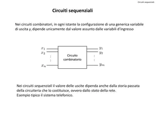
Sequential Logic A sequential circuit is specified by a time sequence of inputs, outputs, and internal states . In contrast, the outputs of combinational logic depend only on the present values of the inputs. It consists of a combinational circuit to which storage elements are connected to form a feedback path.
Sequential Logic The storage elements are devices capable of storing binary information. The binary information stored in these elements at any given time defines the state of the sequential circuit at that time. The sequential circuit receives binary information from external inputs that, together with the present state of the storage elements, determine the binary value of the outputs. These external inputs also determine the condition for changing the state in the storage elements.
Sequential Logic Block diagram of Sequential Logic
Types of sequential circuits Two main types based on function of the timing of their signals. A synchronous sequential circuit is a system whose behavior can be defined from the knowledge of its signals at discrete instants of time. An asynchronous sequential circuit depends upon the input signals at any instant of time and the order in which the inputs change. The storage elements commonly used in asynchronous sequential circuits are time-delay devices.
Synchronous sequential circuit A synchronous sequential circuit employs signals that affect the storage elements at only discrete instants of time. Synchronization is achieved by a timing device called a clock generator, which provides a clock signal having the form of a periodic train of clock pulses . The clock signal is commonly denoted by the identifiers clock and clk . The clock pulses are distributed throughout the system in such a way that storage elements are affected only with the arrival of each pulse. In practice, the clock pulses determine when computational activity will occur within the circuit, and other signals (external inputs and otherwise) determine what changes will take place affecting the storage elements and the outputs.
Synchronous sequential circuit Synchronous sequential circuits that use clock pulses to control storage elements are called clocked sequential circuits and are the type most frequently encountered in practice. They are called synchronous circuits because the activity within the circuit and the resulting updating of stored values is synchronized to the occurrence of clock pulses.
FLIPFLOPS The storage elements (memory) used in clocked sequential circuits are called flipflops. A flip-flop is a binary storage device capable of storing one bit of information.
STORAGE ELEMENTS: LATCHES STORAGE ELEMENTS: LATCHES A storage element in a digital circuit can maintain a binary state indefinitely (as long as power is delivered to the circuit), until directed by an input signal to switch states. The major differences among various types of storage elements are in the number of inputs they possess and in the manner in which the inputs affect the binary state. Storage elements that operate with signal levels (rather than signal transitions) are referred to as latches ; those controlled by a clock transition are flip-flops .
STORAGE ELEMENTS: LATCHES STORAGE ELEMENTS: LATCHES Latches are said to be level sensitive devices; flip-flops are edge-sensitive devices. The two types of storage elements are related because latches are the basic circuits from which all flip-flops are constructed. Although latches are useful for storing binary information and for the design of asynchronous sequential circuits, they are not practical for use as storage elements in synchronous sequential circuits.
SR SR Latch Latch The SR latch is a circuit with two cross-coupled NOR gates or two cross-coupled NAND gates, and two inputs labeled S for set and R for reset. The latch has two useful states. When output Q = 1 and Q = 0, the latch is said to be in the set state. When Q = 0 and Q = 1, it is in the reset state . Outputs Q and Q are normally the complement of each other.
SR SR Latch Latch
SR SR Latch Latch Operation Operation The latch has two useful states. When output Q = 1 and Q = 0, the latch is said to be in the set state . When Q = 0 and Q = 1, it is in the reset state . Outputs Q and Q are normally the complement of each other. However, when both inputs are equal to 1 at the same time, a condition in which both outputs are equal to 0 (rather than be mutually complementary) occurs. If both inputs are then switched to 0 simultaneously, the device will enter an unpredictable or undefined state or a metastable state. Consequently, in practical applications, setting both inputs to 1 is forbidden.
SR SR Latch with Enable Latch with Enable
D D Latch (Transparent Latch) Latch (Transparent Latch) One way to eliminate the undesirable condition of the indeterminate state in the SR latch is to ensure that inputs S and R are never equal to 1 at the same time. If D = 1, the Q output goes to 1, placing the circuit in the set state. If D = 0, output Q goes to 0, placing the circuit in the reset state.
D D Latch (Transparent Latch) Latch (Transparent Latch) The D latch receives that designation from its ability to hold data in its internal storage. It is suited for use as a temporary storage for binary information between a unit and its environment. The binary information present at the data input of the D latch is transferred to the Q output when the enable input is asserted. The output follows changes in the data input as long as the enable input is asserted. This situation provides a path from input D to the output, and for this reason, the circuit is often called a transparent latch.


")
")
")