Altera Tools & Basic Digital Logic Lab Prep Activities
In preparation for the lab, tasks include registering on the Altera website, ordering required boards, installing software, familiarizing with DE0-Nano-SOC board, exploring digital logic concepts, and practicing Verilog circuits like half adder, full adder, D Flip Flop. The activities involve downloading project files, running simulations, writing Verilog code, and creating test benches. A hands-on approach aims to enhance understanding of FPGA tools and basic digital logic.
Download Presentation

Please find below an Image/Link to download the presentation.
The content on the website is provided AS IS for your information and personal use only. It may not be sold, licensed, or shared on other websites without obtaining consent from the author.If you encounter any issues during the download, it is possible that the publisher has removed the file from their server.
You are allowed to download the files provided on this website for personal or commercial use, subject to the condition that they are used lawfully. All files are the property of their respective owners.
The content on the website is provided AS IS for your information and personal use only. It may not be sold, licensed, or shared on other websites without obtaining consent from the author.
E N D
Presentation Transcript
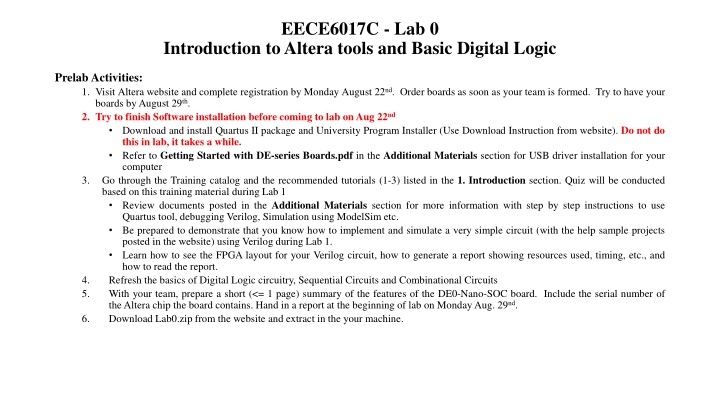
EECE6017C - Lab 0 Introduction to Altera tools and Basic Digital Logic Prelab Activities: 1. Visit Altera website and complete registration by Monday August 22nd. Order boards as soon as your team is formed. Try to have your boards byAugust 29th. 2. Try to finish Software installation before coming to lab onAug 22nd Download and install Quartus II package and University Program Installer (Use Download Instruction from website). Do not do this in lab, it takes a while. Refer to Getting Started with DE-series Boards.pdf in the Additional Materials section for USB driver installation for your computer 3. Go through the Training catalog and the recommended tutorials (1-3) listed in the 1. Introduction section. Quiz will be conducted based on this training material during Lab 1 Review documents posted in the Additional Materials section for more information with step by step instructions to use Quartus tool, debugging Verilog, Simulation using ModelSim etc. Be prepared to demonstrate that you know how to implement and simulate a very simple circuit (with the help sample projects posted in the website) using Verilog during Lab 1. Learn how to see the FPGA layout for your Verilog circuit, how to generate a report showing resources used, timing, etc., and how to read the report. 4. Refresh the basics of Digital Logic circuitry, Sequential Circuits and Combinational Circuits 5. With your team, prepare a short (<= 1 page) summary of the features of the DE0-Nano-SOC board. Include the serial number of theAltera chip the board contains. Hand in a report at the beginning of lab on MondayAug. 29nd. 6. Download Lab0.zip from the website and extract in the your machine.
EECE6017C - Lab 0 Introduction to Altera tools and Basic Digital Logic Work to be done during this lab: 1. Download the project halfadder.zip from website and try to run and simulate the 1-bit Half Adder. The Verilog Test bench files and the Vector Waveform File are present in the project folder for your review. (Refer to the documents Simulation of Verilog Designs using ModelSim Graphical Waveform Editor and Using ModelSim to simulate Logic Circuits posted in the Additional materials section in the website) 2. Download the project fulladder.zip. A skeleton for the full adder module is given and the task is to try complete the Full adder (using half adder module explained in 1). Simulate and show the result in the waveform editor and the associated test bench file 3. Download the project dfipflop.zip and simulate a D Flip flop Verilog module. The project has the Verilog code included. Task is to use the Waveform Editor to show results graphically and generate test bench file. 4. Download mux2to1.zip and simulate the module and test bench files. 5. Turn in the code, test bench and report for Full adder and Test bench file for D Flip Flop circuit
1. Half Adder Ahalf adder is a circuit that receives two 1-bit inputs and adds them together to generate a 1-bit result (sum) and a 1-bit carry. The basic building blocks (gates) of a half adder consist of an XOR gate and an AND gate. Start the design process by creating a truth table, showing all possible input combinations and writing down the expected output states. Verilog Code note comments, indentation: //module for halfadder //input bits a,b; output bits sum, carry //designed by YOURNAME on THISDATE module halfadder(a,b,sum,carry); input a,b; output sum, carry; assign sum = a^b; // sum bit assign carry = (a&b) ; //carry bit endmodule
Test Bench (half adder) //testbench for halfadder //input bits a,b; output bits sum, carry //designed by YOURNAME on THISDATE `timescale 1 ps/ 1 ps module halfadder_vlg_vec_tst(); // general purpose registers reg a; reg b; // wires wire carry; wire sum; // assign statements (if any) halfadder testunit ( // port map - connection between master ports and signals/registers .a(a), .b(b), .carry(carry), .sum(sum) ); initial begin #400 $stop; end // a always begin a = 1'b0; a = #200 1'b1; #200; end // b always begin b = 1'b0; b = #100 1'b1; #100; end endmodule
2. Full Adder Using the half adder example, Write the Verilog code for a Full Adder, that takes in three 1-bit inputs, a, b and carryin, and gives sum and carryout 1-bit outputs. Write the code for a test bench for the adder, and give appropriate inputs to test all possible combinations. Verilog Code: //module for fulladder //input bits a,b,cin; output bits sum, carry //designed by YOURNAME on THISDATE module fulladder(a,b,cin,sum,carry); input a,b,cin; output sum, carry; - Enter Code here endmodule
3. D Flip Flop (Delay) The D type flip-flop has one data input 'D' and a clock input. The circuit edge triggers on the clock input. The flip-flop also has two outputs Q and Q' (where Q' is the reverse of Q). The operation of the D type flip-flop is as follows: Any input appearing (present state at t) at the input D, will be produced at the output Q in time t+1 (next state). e.g. if in the present state, we have D = 0 and Q = 1, the next state will be D = x and Q = 0 (previous state). The positive edge triggered D flip-flop can be modeled using behavioral modeling as shown below. Verilog Code: //module for D flipflop //input bits D,CLK (clock); output bits Q,Qi (Q-inverse) //designed by YOURNAME on THISDATE module dflipflop(D, Clk, Q, Qi); output Q,Qi; input D, Clk; reg Q,Qi; initial begin Q=1'b0; Qi=1'b1; end always @ (posedge Clk) begin Q=D; Qi=~D; end endmodule
4. 2 to 1 MUX A 2-to-1 multiplexer has two inputs D0 and D1, one select input S and one output Y. Since there are two input signals only two ways are possible to connect the inputs to the outputs, so one select is needed to do these operations. Depending on the selector switching the inputs are produced at outputs , i.e., D0 , D1 and are switched to the output for S=0 and S=1 respectively . With the truth table for 2 to 1 multiplexer and write a test bench for the given mux Verilog module. Corresponding expression for mux output Y is given below The Verilog code can also be written using case statements or by simply using conditional operator (?: ) with assign statement. Verilog Code: //module for 2-to-1 mux //input bits D0,D1,S(select); output bit Y //designed by YOURNAME on THISDATE module mux2to1( D0 , D1 , S, Y); input D0, D1, S; output Y; reg Y; always @ (S or D0 or D1) endmodule begin end SELECT (S) IN1 (D0) IN2 (D1) OUT (Y) if (S == 1'b0) begin end else begin end Y = D0; 0 0 X 0 (D0) 0 1 X 1 (D0) Y = D1; 1 X 1 1 (D1) 1 X 0 0 (D1)
Example: an altera state machine design: what does the state diagram look like? Draw the transition diagram Verilog Code: //module for state machine //input bits clk (clock), in, reset; //output 4-bit value out //designed by YOURNAME on THISDATE module statem(clk, in, reset, out); input clk, in, reset; output [3:0] out; reg [3:0] out; reg [1:0] state; parameter zero=0, one=1, two=2, three=3; always @(state) begin case (state) zero: out = 4'b0000; one: out = 4'b0001; two: out = 4'b0010; three: out = 4'b0100; default: out = 4'b0000; endcase end end endmodule always @(posedge clk or posedge reset) begin if (reset) state = zero; else case (state) zero: state = one; one: if (in) state = zero; else state = two; two: state = three; three: state = zero; endcase 8
Points to remember while implementing: When creating a new project, be sure to select the correct device under the Available device list in the Picture shown here. The Device you need to select is 5CSEMA4U23C6. Use the name filter to select the device you want
To use RTL viewer Goto Tool - > Netlist Viewers -> RTL Viewer
Waveform Editor - Simulation The Quartus II software also allows you to generate the following types of output files for use in performing functional and timing simulation in EDA simulation tools: You can create Verilog Test Bench Files (.vt) and VHDL Test Bench Files (.vht) for use with EDA simulation tools from a Vector Waveform File (.vwf) in the Quartus II Waveform Editor, using Simulation menu Generate ModelSim Testbench and script . Verilog HDL and VHDL Test Bench Files are test bench template files that contain an instantiation of the top-level design file and test vectors from the Vector Waveform File. You can also generate self-checking test bench files if you specify the expected values in the Vector Waveform File. To open Waveform Editor File ->New. The New file wizard will appear as shown in the picture Select University Program VWF under the Verification/Debugging Files The Simulation Waveform Editor is shown in the right.
Using Waveform Editor Picture below is Simulation Waveform editor in the Quartus and simulation results Refer to Simulation of Verilog Designs Using ModelSim Graphical Waveform Editor in the Additional materials Tips: 1. Set the simulation time using Edit->Set End time 2. Set Grid Size using Edit->Grid Size, In this example total simulation time is 400us and Grid Size is 100us. 3. Select the Input a or b and Edit->Radix->Binary 4. Select input a, and to configure the waveform for a, Edit->Value->Count Value. Set Count time, say 200 ms 5. Similarly for input b, Set the Count time, say 100 ms 6. Run Simulation and you can see the resulting waveform for all the possible outcomes 7. This tool will help to automatically generate the test bench script. See example\simulation\modelsim folder and Waveform.vwf.vt is the test vector file automatically generated.
Homework Design and test the following combinational logic structures using behavioral modeling. 1. Using the example done in lab0, Write the Verilog code for a 4-bit Adder, that takes in three inputs, A[3:0], B[3:0] and 1-bit Carry-in, and gives Result[3:0] and Carryout 1-bit. Write the code for a test bench for the adder, and give appropriate inputs to test all possible combinations. This module will be a basic building block for next lab exercise. 2. Create a 4-bit Shifter with one 4 bit input, 2 bit Select value (00 Shift LEFT, 10 Shift Right, 11 Shift Right Arithmetic) and 4 bit Output value 3. (sequential logic) Give the state table and the transition diagram for the state machine on slide 8.
