Characteristics of Instrumentation Amplifiers
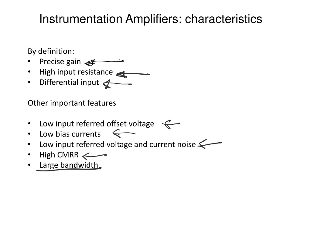

Instrumentation Amplifiers: characteristics
By definition:
•
Precise gain
•
High input resistance
•
Differential input
Other important features
•
Low input referred offset voltage
•
Low bias currents
•
Low input referred voltage and current noise
•
High CMRR
•
Large bandwidth


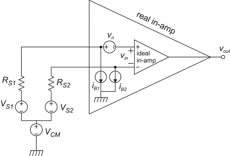
Instrumentation Amplifiers: connection to the
source


Balanced case
(R
S1
=R
S2
=R
S
)

Offset: v
n
=v
io
, i
B1
-i
B2
=I
B1
-I
B2
=I
io
Noise: v
n
and i
n1
, i
n2
are represented by their PSD
(power spectral density)
cross-spectrum
If
i
b1
and
i
b2
are uncorrelated and their PSD is S
I
:
Monolithic In-Amps
Typical pin configuration
Function of the SENSE
terminal
Input and output offset / noise
Typical two-stage architecture of In-amps
Generally, A
2
= 1, thus:
Three-opamp instrumentation amplifier
The circuit that provides
V
REF
must have a very low
output resistance (<<R)
Mismatch of these resistors
degrades the CMRR of the
second stage. Resistor
trimming is necessary for
CMRRs > 60 dB
I
n
s
t
r
u
m
e
n
t
a
t
i
o
n
A
m
p
l
i
f
i
e
r
s
A
D
6
2
0
At G≥100 the
amplifier BW is
larger than 100kHz.
The noise density
starts to fall for
f> 100kHz
The RTI noise
decreases with G
A
D
6
2
0
Nearly constant GBW product: BW determined by first stage
GBW does not increase much beyond the G=10 case: BW affected by second stage
O
u
t
p
u
t
n
o
i
s
e
>
>
i
n
p
u
t
n
o
i
s
e
Broad-Band Noise: √S
BB
Low Frequency Noise
Integrated over 0.1-10 Hz
Broad-Band Noise: √S
BB
Low Frequency Noise
Integrated over 0.1-10 Hz
Current
Slew -Rate
Settling times
A
D
6
2
0
Input offset
Output offset
The effective input referred offset (RTI)
is a combination of the input and output offset
Such a small offset voltage and offset drift is
the result of a laser-trimmed resistor-load
BJT input pair
The input bias current and input offset current are similar, since
such a small bias current is the result of internal bias current cancellation
The AD 620 in-amp represent a good trade-off between input noise
voltage, input bias currents and supply current (quiescent current)
A
D
8
4
2
9
The AD8429 has a much smaller input referred noise than the AD620
(BB-noise) ……..
..... but its input current noise is much larger..
A
D
8
4
2
9
The bias current (dc value) is also much larger than AD620 one
The AD8429 is faster than the AD620
…. but it requires much more quiescent current
I
n
s
t
r
u
m
e
n
t
a
t
i
o
n
A
m
p
l
i
f
i
e
r
s
The INA333 is a very low-power
instrumentation amplifier
(I
supply
: 50
A)
As a result, its input referred
voltage noise is larger and its
bandwidth smaller.
I
N
A
3
3
3
Very low input bias current
Small bandwidths
Large noise density
AD620 was 9 nV/√Hz
I
N
A
1
1
1
:
J
-
F
e
t
i
n
p
u
t
Note the presence of a
sense (Feedback) terminal in
the 16 pin case
Offset is considerably worse than
AD620 which has a BJT input stage
I
N
A
1
1
1
…. but the (integrated) low-frequency
voltage noise is much worse (was 0.28
V) in
the AD 620
The broad-band input referred noise density
is similar to AD 620 …..
The strong advantage of a JFET input is the
negligible noise current density
The LTC 1100 uses an Autozero
technique to cancel the input offset and
flicker noise.
The side-effect is foldover, resulting in an
increased low-frequency noise density.
Instrumentation amplifiers are known for their precise gain, high input resistance, differential input, and low offset voltage. They offer features like low bias currents, noise, high CMRR, and large bandwidth. Learn about their connection to the source, offset, noise characteristics, monolithic in-amps, input/output offset noise, and three-opamp configurations. Delve into specific models like AD620 and understand their key parameters affecting performance.

Download Presentation

Please find below an Image/Link to download the presentation.
The content on the website is provided AS IS for your information and personal use only. It may not be sold, licensed, or shared on other websites without obtaining consent from the author.If you encounter any issues during the download, it is possible that the publisher has removed the file from their server.
You are allowed to download the files provided on this website for personal or commercial use, subject to the condition that they are used lawfully. All files are the property of their respective owners.
The content on the website is provided AS IS for your information and personal use only. It may not be sold, licensed, or shared on other websites without obtaining consent from the author.
E N D
Presentation Transcript
Instrumentation Amplifiers: characteristics By definition: Precise gain High input resistance Differential input Other important features Low input referred offset voltage Low bias currents Low input referred voltage and current noise High CMRR Large bandwidth
Instrumentation Amplifiers: connection to the source ( ) = = + = v V i R v V i R V V v 1 1 1 2 2 2 1 2 in S B S n i R S B S S S nt v v i R 1 1 2 2 nt n B S B S ( ) Balanced case (RS1=RS2=RS) = + v v R i i 1 2 nt n S B B
Offset: vn=vio, iB1-iB2=IB1-IB2=Iio ( B S io iot I R v v + = 1 ) = + I v R I 2 B io S io Noise: vnand in1, in2are represented by their PSD (power spectral density) cross-spectrum ( ) = + + 2 S 2 S S R S S S 1 2 1 2 vnt vn I I I I If ib1and ib2are uncorrelated and their PSD is SI: = + 2 2 S S R S vnt vn S I
Monolithic In-Amps ( ) = + V G V V V + out IN IN REF Typical pin configuration Function of the SENSE terminal
Input and output offset / noise Typical two-stage architecture of In-amps Generally, A2= 1, thus: v v = + = + 2 2 n n v v v 1 1 nRTI n n A G 1
Three-opamp instrumentation amplifier Mismatch of these resistors degrades the CMRR of the second stage. Resistor trimming is necessary for CMRRs > 60 dB The circuit that provides VREFmust have a very low output resistance (<<R) 2 R = 1+ 1 G R G
Instrumentation Amplifiers AD 620 ( ) = + V G + V V / V + out IN 4 . IN R REF = 1 49 G k G The RTI noise decreases with G At G 100 the amplifier BW is larger than 100kHz. The noise density starts to fall for f> 100kHz
AD 620 GBW does not increase much beyond the G=10 case: BW affected by second stage Nearly constant GBW product: BW determined by first stage Slew -Rate Settling times Output noise >> input noise Broad-Band Noise: SBB Low Frequency Noise Integrated over 0.1-10 Hz Broad-Band Noise: SBB Current Low Frequency Noise Integrated over 0.1-10 Hz
Such a small offset voltage and offset drift is the result of a laser-trimmed resistor-load BJT input pair AD 620 The effective input referred offset (RTI) is a combination of the input and output offset Input offset Output offset The input bias current and input offset current are similar, since such a small bias current is the result of internal bias current cancellation The AD 620 in-amp represent a good trade-off between input noise voltage, input bias currents and supply current (quiescent current)
AD 8429 The AD8429 has a much smaller input referred noise than the AD620 (BB-noise) .. ..... but its input current noise is much larger..
AD 8429 The bias current (dc value) is also much larger than AD620 one The AD8429 is faster than the AD620 . but it requires much more quiescent current
Instrumentation Amplifiers The INA333 is a very low-power instrumentation amplifier (Isupply: 50 A) As a result, its input referred voltage noise is larger and its bandwidth smaller.
INA 333 Small bandwidths Very low input bias current Large noise density AD620 was 9 nV/ Hz
INA 111: J-Fet input Note the presence of a sense (Feedback) terminal in the 16 pin case Offset is considerably worse than AD620 which has a BJT input stage
INA 111 . but the (integrated) low-frequency voltage noise is much worse (was 0.28 V) in the AD 620 The broad-band input referred noise density is similar to AD 620 .. The strong advantage of a JFET input is the negligible noise current density
The LTC 1100 uses an Autozero technique to cancel the input offset and flicker noise. The side-effect is foldover, resulting in an increased low-frequency noise density.