ARM Timer Programming: MSP432 Chapter 5

 undefined
Chapter 5
MSP432 ARM Timer Programming
1


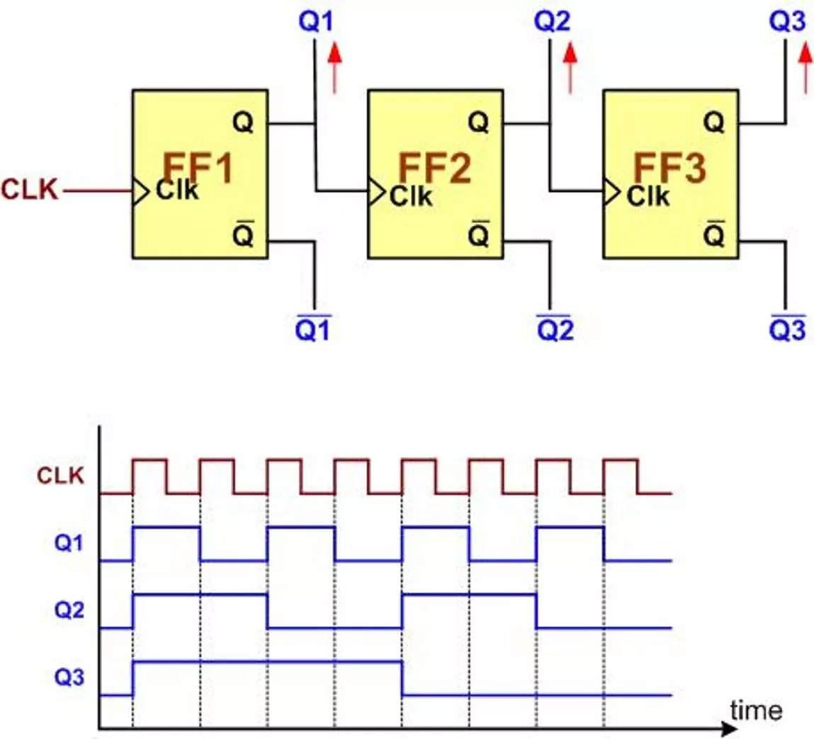
A 3-bit Counter
2
An 8-bit up-counter stages
3
An 8-bit down-counter stages
4
Counting Events Using a Counter
5
Using Counter as a Timer
6
Capturing
7
System Tick Timer Internal Structure
8
STCTRL (System Tick Control)
9
System Tick Counting
10
STRVR vs. STCVR
11
System Tick Timer Internal Structure
12
Timer32 Registers
13
T32CONTROLxRegister
14
Counting in Free-Running Mode vs. Periodic
Mode
15
T32RIS Register
16
T32LOAD vs. T32VALUE
17
The Timer32 Prescaler
18
Timer_A Simplified Diagram
19
A more detailed diagram of Timer_A
20
TAxR register
21
TAxCTL register
22
TAxCTL register
23
TAxCCRn Registers and TAxCCTLn Flags
24
TAxCCRn Register
25
TAxCCTLn Register
26
TAxCCTLn Register (Table 17-6 of the chip
manual)
27
TAxCCTLn Register (Table 17-6 of the chip
manual) (Cont.)
28
TAxCCTLn Register (Table 17-6 of the chip
manual) (Cont.)
29
TAxEXn Register
30
Counting in Up Mode
31
Clock in Timer_A
32
Continuous mode
33
Input Edge Time Capturing
34
TAxCCTLn Register
35
TAxCCTLn Register (Table 17-6 of the chip
manual)
36
TAxCCTLn Register (Table 17-6 of the chip
manual) (Cont.)
37
TAxCCTLn Register (Table 17-6 of the chip
manual) (Cont.)
38
Choosing the Capture Edge
39
Port pin assignement of Timer_A
40
Measuring Period and Pulse Width
41
Delve into the world of ARM Timer Programming with MSP432 in Chapter 5. Explore topics such as 3-bit counters, 8-bit up and down counters, counting events, using counters as timers, system tick timers, control registers, interrupt handling, and more.

Download Presentation

Please find below an Image/Link to download the presentation.
The content on the website is provided AS IS for your information and personal use only. It may not be sold, licensed, or shared on other websites without obtaining consent from the author.If you encounter any issues during the download, it is possible that the publisher has removed the file from their server.
You are allowed to download the files provided on this website for personal or commercial use, subject to the condition that they are used lawfully. All files are the property of their respective owners.
The content on the website is provided AS IS for your information and personal use only. It may not be sold, licensed, or shared on other websites without obtaining consent from the author.
E N D
Presentation Transcript
Chapter 5 MSP432 ARM Timer Programming 1
Timer32 Registers Offset 00H 04H Acronym T32LOAD1 T32VALUE1 T32CONTROL 1 T32INTCLR1 T32RIS1 T32MIS1 T32BGLOAD1 T32LOAD2 T32VALUE2 T32CONTROL 2 T32INTCLR2 T32RIS2 T32MIS2 T32BGLOAD2 Register Name Timer 1 Load Register Timer 1 Current Value Register Type RW R Reset Value 0 FFFFFFFFH 08H Timer 1 Timer Control Register RW 20H 0CH 10H 14H 18H 20H 24H Timer 1 Interrupt Clear Register Timer 1 Raw Interrupt Status Register Timer 1 Interrupt Status Register Timer 1 Background Load Register Timer 2 Load Register Timer 2 Current Value Register W R R RW RW R - 0 0 0 0 FFFFFFFFH 28H Timer 2 Timer Control Register RW 20H 2CH 30H 34H 38H Timer 2 Interrupt Clear Register Timer 2 Raw Interrupt Status Register Timer 2 Interrupt Status Register Timer 2 Background Load Register W R R RW - 0 0 0H 13
TAxCTL register bit Name Description Timer_A Interrupt Flag 0: Timer did not overflow 1: Timer overflowed Timer_A Interrupt Enable (0: Disabled, 1: Enabled) Timer_A Clear Mode Control: 00: Stop mode: timer is halted 01: Up mode: Timer counts up to TAxCCR0 10: Continuous mode: Timer counts up to 0xFFFF 11: Up/down mode: Timer counts up to TAxCCR0 then down to 0. Input divider: These bits select the divider for the input clock: 00: divide by 1 01: divide by 2 10: divide by 4 11: divide by 8 Timer_A clock Source Select: These bits select the Timer_A clock source: 00: TAxCLK (external clock): The timer uses external clock which is fed to the PM_TAxCLK pin. 01: ACLK (internal clock) 10: SMCLK (internal clock) 11: INCLK 0 TAIFG 1 2 TAIE TACLR 4-5 MC 6-7 ID 23 8-9 TASSEL
TAxCCTLn Register (Table 17-6 of the chip manual) bit Name Description Capture mode 00: No capture 01: Capture on rising edge 10: Capture on falling edge 11: Capture on both rising and falling edges Capture/compare input select. These its select the TAxCCR0 input signal: 00: CCIxA 01: CCIxB 10: GND 11: VCC Synchronize capture source. This bit is used to synchronize the capture input signal with the timer clock. 0: Asynchronous capture 1: Synchronous capture 15-14 CM 13-12 CCIS 11 SCS 27
TAxCCTLn Register (Table 17-6 of the chip manual) (Cont.) bit Name Description Synchronized capture/compare input. The selected CCI input signal is latched with the EQUx signal and can be read via this bit. Capture mode 0: Compare mode 1: Capture mode Output mode. Modes 2, 3, 6, and 7 are not useful for TAxCCR0 because EQUx = EQU0 000: OUT bit value 001: Set 010: Toggle/reset 011: Set/reset 100: Toggle 101: Reset 110: Toggle/set 111: Reset/set 10 SCCI 8 CAP OUTMO D 7-5 28
TAxCCTLn Register (Table 17-6 of the chip manual) (Cont.) bit Name Description Capture/compare interrupt enable. This bit enables the interrupt request of the corresponding CCIFG flag. 0: Interrupt disabled 1: Interrupt enabled Capture/compare input. The selected input signal can be read by this bit. Output. For output mode 0, this bit directly controls the state of the output. 0: Output low 1: Output high Capture overflow. This bit indicates a capture overflow occurred. COV must be reset with software. 0: No capture overflow occurred 1: Capture overflow occurred Capture/compare interrupt flag 0: No interrupt pending 1: interrupt pending 4 CCIE 3 CCI 2 OUT 1 COV 0 CCIFG 29
TAxCCTLn Register (Table 17-6 of the chip manual) bit Name Description Capture mode 00: No capture 01: Capture on rising edge 10: Capture on falling edge 11: Capture on both rising and falling edges Capture/compare input select. These its select the TAxCCR0 input signal: 00: CCIxA 01: CCIxB 10: GND 11: VCC Synchronize capture source. This bit is used to synchronize the capture input signal with the timer clock. 0: Asynchronous capture 1: Synchronous capture 15-14 CM 13-12 CCIS 11 SCS 36
TAxCCTLn Register (Table 17-6 of the chip manual) (Cont.) bit Name Description Synchronized capture/compare input. The selected CCI input signal is latched with the EQUx signal and can be read via this bit. Capture mode 0: Compare mode 1: Capture mode Output mode. Modes 2, 3, 6, and 7 are not useful for TAxCCR0 because EQUx = EQU0 000: OUT bit value 001: Set 010: Toggle/reset 011: Set/reset 100: Toggle 101: Reset 110: Toggle/set 111: Reset/set 10 SCCI 8 CAP OUTM OD 7-5 37
TAxCCTLn Register (Table 17-6 of the chip manual) (Cont.) bit Name Description Capture/compare interrupt enable. This bit enables the interrupt request of the corresponding CCIFG flag. 0: Interrupt disabled 1: Interrupt enabled Capture/compare input. The selected input signal can be read by this bit. Output. For output mode 0, this bit directly controls the state of the output. 0: Output low 1: Output high Capture overflow. This bit indicates a capture overflow occurred. COV must be reset with software. 0: No capture overflow occurred 1: Capture overflow occurred Capture/compare interrupt flag 0: No interrupt pending 1: interrupt pending 4 CCIE 3 CCI 2 OUT 1 COV 0 CCIFG 38
Choosing the Capture Edge CM Capture mode 00 No capture 01 Capture on rising edge 10 Capture on falling edge 11 Capture on both edges 39
Port pin assignement of Timer_A Timer_A Port Pin Timer_A Port Pin Timer_A Port Pin Timer_A Port Pin TA0.0 TA0.1 TA0.2 TA0.3 TA0.4 P7.3 P2.4 P2.5 P2.6 P2.7 TA1.0 TA1.1 TA1.2 TA1.3 TA1.4 P8.0 P7.7 P7.6 P7.5 P7.4 TA2.0 TA2.1 TA2.2 TA2.3 TA2.4 P8.1 P5.6 P5.7 P6.6 P6.7 TA3.0 TA3.1 TA3.2 TA3.3 TA3.4 P10.4 P10.5 P8.2 P9.2 P9.3 40


")