Computer Architecture and Design: Basic Organization and Operation


Computer
Architecture
Chapter
Six
Basic Computer
Organization
and
Design
A
f
t
e
r
t
h
e
f
e
t
c
h
a
n
d
d
e
c
o
d
e
p
h
a
s
e
,
P
C
c
o
n
t
a
i
n
s
3
1
,
w
h
i
c
h
i
s
t
h
e
a
d
d
r
e
s
s
o
f
t
h
e
n
e
x
t
i
n
s
t
r
u
c
t
i
o
n
i
n
t
h
e
p
r
o
g
r
a
m
(
t
h
e
r
e
t
u
r
n
a
d
d
r
e
s
s
)
.
T
h
e
r
e
g
i
s
t
e
r
A
R
h
o
l
d
s
t
h
e
e
f
f
e
c
t
i
v
e
a
d
d
r
e
s
s
1
7
0
[
s
e
e
f
i
g
u
r
e
6
.
1
0
(
a
)
]
.
T
h
e
B
S
A
i
n
s
t
r
u
c
t
i
o
n
p
e
r
f
o
r
m
s
t
h
e
f
o
l
l
o
w
i
n
g
n
u
m
e
r
i
c
a
l
o
p
e
r
a
t
i
o
n
:
M[170] ← 31,
PC
←
170
+ 1
=171
T
h
e
r
e
s
u
l
t
o
f
t
h
i
s
o
p
e
r
a
t
i
o
n
i
s
s
h
o
w
n
i
n
f
i
g
u
r
e
6
.
1
0
(
b
)
.
T
h
e
r
e
t
u
r
n
a
d
d
r
e
s
s
(
3
1
)
i
s
s
t
o
r
e
d
i
n
m
e
m
o
r
y
l
o
c
a
t
i
o
n
1
7
0
a
n
d
c
o
n
t
r
o
l
c
o
n
t
i
n
u
e
s
w
i
t
h
t
h
e
s
u
b
r
o
u
t
i
n
e
p
r
o
g
r
a
m
s
t
a
r
t
i
n
g
f
r
o
m
a
d
d
r
e
s
s
1
7
1
.
To return to the original program
(at
address 31), this is
accomplished by means
of an
indirect
BUN
instruction placed at the
end of
the
subroutine.
W
h
e
n
B
U
N
i
s
e
x
e
c
u
t
e
d
,
c
o
n
t
r
o
l
g
o
e
s
t
o
t
h
e
i
n
d
i
r
e
c
t
p
h
a
s
e
t
o
r
e
a
d
t
h
e
e
f
f
e
c
t
i
v
e
a
d
d
r
e
s
s
a
t
l
o
c
a
t
i
o
n
1
7
0
,
w
h
e
r
e
i
t
f
i
n
d
s
t
h
e
p
r
e
v
i
o
u
s
l
y
s
a
v
e
d
a
d
d
r
e
s
s
3
1
.
T
h
e
n
t
h
e
e
f
f
e
c
t
i
v
e
a
d
d
r
e
s
s
3
1
i
s
t
r
a
n
s
f
e
r
r
e
d
t
o
P
C
.
T
h
e
n
e
x
t
i
n
s
t
r
u
c
t
i
o
n
c
y
c
l
e
f
i
n
d
s
P
C
w
i
t
h
t
h
e
v
a
l
u
e
3
1
,
s
o
c
o
n
t
r
o
l
c
o
n
t
i
n
u
e
s
t
o
e
x
e
c
u
t
e
t
h
e
i
n
s
t
r
u
c
t
i
o
n
a
t
t
h
e
r
e
t
u
r
n
a
d
d
r
e
s
s
.
I
S
Z
(
I
n
c
r
e
m
e
n
t
a
n
d
S
k
i
p
i
f
Z
e
r
o
)
I
n
s
t
r
u
c
t
i
o
n
This
instruction increments the
word
specified by the effective
address,
and
if the result is zero,
PC
is incremented
by one.
When
PC
is incremented
by one,
the
next
instruction in the sequence is
skipped.
T
h
e
m
i
c
r
o
o
p
e
r
a
t
i
o
n
s
n
e
e
d
e
d
t
o
e
x
e
c
u
t
e
t
h
e
I
S
Z
i
n
s
t
r
u
c
t
i
o
n
a
r
e
:
25-50
Yacoup
K.
Hanna

26-50
Yacoup
K.
Hanna
Computer
Architecture
Chapter
Six
Basic Computer
Organization
and
Design
D
6
T
4
:
D
6
T
5
:
D
6
T
6
:
DR ← M
[AR]
DR ← DR +
1
M
[AR]
←
DR,
if (DR =
0)
then (PC ← PC + 1), SC ←
0
The
operation
decoder
D
6
is
active
when
the
instruction
has
an
ISZ
operation whose binary
code value
is
110.
T
o
e
x
e
c
u
t
e
t
h
e
I
S
Z
i
n
s
t
r
u
c
t
i
o
n
,
t
h
r
e
e
t
i
m
i
n
g
s
i
g
n
a
l
s
a
r
e
n
e
e
d
e
d
:
-
1.
The
clock transition associated
with
timing signal
T
4
read the
memory
into
DR
.
2.
The
clock
transition
associated
with
timing
signal
T
5
increments
DR.
3.
The
clock transition associated
with
timing signal
T
6
store the
word
back
into memory.
In the same clock transition,
SC
is
cleared to 0
which
transfers the control to timing signal
T
0
to start
a new instruction
cycle.
7.
I
n
p
u
t
-
O
u
t
p
u
t
a
n
d
I
n
t
e
r
r
u
p
t
C
o
m
p
u
t
e
r
s
y
s
t
e
m
s
i
n
c
l
u
d
e
m
a
n
y
t
y
p
e
s
o
f
i
n
p
u
t
a
n
d
o
u
t
p
u
t
d
e
v
i
c
e
s
.
T
o
d
e
m
o
n
s
t
r
a
t
e
t
h
e
m
o
s
t
b
a
s
i
c
r
e
q
u
i
r
e
m
e
n
t
s
f
o
r
i
n
p
u
t
a
n
d
o
u
t
p
u
t
c
o
m
m
u
n
i
c
a
t
i
o
n
,
a
t
e
r
m
i
n
a
l
u
n
i
t
w
i
t
h
a
k
e
y
b
o
a
r
d
a
n
d
p
r
i
n
t
e
r
u
s
e
d
f
o
r
t
h
i
s
i
l
l
u
s
t
r
a
t
i
o
n
.
1.
I
n
p
u
t
-
O
u
t
p
u
t
C
o
n
f
i
g
u
r
a
t
i
o
n
We
mentioned before that the terminals send
and receive
serial
information. Each
type
of this information has eight bits of
an
alphanumeric code.
The
serial information from the keyboard shifted
into the input register
INPR
. The
serial information for the printer is
stored
in
the output register
OUTR
.
The two
registers
INPR &
OUTR
communicate
with an
interface
serially, and with
an accumulator
AC
in
parallel.
Figure 6.11
shows
the input-output configuration. Where the
transmitter interface
receives
serial information from the keyboard and
transmits it to
INPR,
while
the
receiver
interface receives information
from
OUTR
and
sends
it
serially
to
the
printer
.
Computer
Architecture
Chapter
Six
Basic Computer
Organization
and
Design
T
h
e
i
n
p
u
t
a
n
d
o
u
t
p
u
t
r
e
g
i
s
t
e
r
s
I
N
P
R
&
O
U
T
R
r
e
s
p
e
c
t
i
v
e
l
y
a
r
e
8
-
b
i
t
s
.
T
h
e
y
h
o
l
d
a
l
p
h
a
n
u
m
e
r
i
c
i
n
f
o
r
m
a
t
i
o
n
.
T
h
e
i
n
p
u
t
a
n
d
o
u
t
p
u
t
f
l
a
g
s
F
G
I
&
F
G
O
a
r
e
1
-
b
i
t
c
o
n
t
r
o
l
f
l
i
p
-
f
l
o
p
s
.
T
h
e
f
l
a
g
F
G
I
i
s
s
e
t
t
o
1
w
h
e
n
n
e
w
i
n
f
o
r
m
a
t
i
o
n
i
s
a
v
a
i
l
a
b
l
e
i
n
t
h
e
i
n
p
u
t
d
e
v
i
c
e
a
n
d
i
s
c
l
e
a
r
e
d
t
o
0
w
h
e
n
t
h
e
i
n
f
o
r
m
a
t
i
o
n
i
s
a
c
c
e
p
t
e
d
b
y
t
h
e
c
o
m
p
u
t
e
r
.
F
i
g
u
r
e
6
.
1
1
27-50
Yacoup
K.
Hanna
T
r
a
n
s
f
e
r
o
f
i
n
f
o
r
m
a
t
i
o
n
f
r
o
m
t
h
e
k
e
y
b
o
a
r
d
t
o
t
h
e
c
o
m
p
u
t
e
r
I
n
i
t
i
a
l
l
y
t
h
e
i
n
p
u
t
f
l
a
g
F
G
I
i
s
c
l
e
a
r
e
d
t
o
0
.
W
h
e
n
a
k
e
y
i
s
s
t
r
u
c
k
i
n
t
h
e
k
e
y
b
o
a
r
d
,
a
n
8
-
b
i
t
a
l
p
h
a
n
u
m
e
r
i
c
c
o
d
e
i
s
s
h
i
f
t
e
d
i
n
t
o
I
N
P
R
a
n
d
t
h
e
i
n
p
u
t
f
l
a
g
F
G
I
i
s
s
e
t
t
o
1
.
A
s
l
o
n
g
a
s
t
h
e
f
l
a
g
i
s
s
e
t
,
t
h
e
i
n
f
o
r
m
a
t
i
o
n
i
n
I
N
P
R
c
a
n
n
o
t
b
e
c
h
a
n
g
e
d
b
y
s
t
r
i
k
i
n
g
a
n
o
t
h
e
r
k
e
y
.
T
h
e
c
o
m
p
u
t
e
r
c
h
e
c
k
s
t
h
e
f
l
a
g
b
i
t
;
i
f
i
t
i
s
1
,
t
h
e
i
n
f
o
r
m
a
t
i
o
n
f
r
o
m
I
N
P
R
i
s
t
r
a
n
s
f
e
r
r
e
d
i
n
p
a
r
a
l
l
e
l
i
n
t
o
A
C
a
n
d
F
G
I
i
s
c
l
e
a
r
e
d
t
o
0
.
O
n
c
e
t
h
e
f
l
a
g
c
l
e
a
r
e
d
,
n
e
w
i
n
f
o
r
m
a
t
i
o
n
s
h
i
f
t
e
d
i
n
t
o
I
N
P
R
b
y
s
t
r
i
k
i
n
g
a
n
o
t
h
e
r
k
e
y
.
T
r
a
n
s
f
e
r
o
f
i
n
f
o
r
m
a
t
i
o
n
f
r
o
m
t
h
e
c
o
m
p
u
t
e
r
t
o
t
h
e
p
r
i
n
t
e
r
The
output register
OUTR
works
similar to
INPR,
but
the direction
of
information flow
reversed.
I
n
i
t
i
a
l
l
y
t
h
e
o
u
t
p
u
t
f
l
a
g
F
G
O
i
s
s
e
t
t
o
1
.
T
h
e
c
o
m
p
u
t
e
r
c
h
e
c
k
s
t
h
e
o
u
t
p
u
t
f
l
a
g
;
i
f
i
t
i
s
1
,
t
h
e
i
n
f
o
r
m
a
t
i
o
n
f
r
o
m
A
C
i
s
t
r
a
n
s
f
e
r
r
e
d
i
n
Computer
Architecture
Chapter
Six
Basic Computer
Organization
and
Design
p
a
r
a
l
l
e
l
t
o
O
U
T
R
a
n
d
F
G
O
i
s
c
l
e
a
r
e
d
t
o
0
.
T
h
e
o
u
t
p
u
t
d
e
v
i
c
e
a
c
c
e
p
t
s
t
h
e
c
o
d
e
d
i
n
f
o
r
m
a
t
i
o
n
,
p
r
i
n
t
s
t
h
e
c
o
r
r
e
s
p
o
n
d
i
n
g
c
h
a
r
a
c
t
e
r
,
a
n
d
w
h
e
n
t
h
e
o
p
e
r
a
t
i
o
n
i
s
c
o
m
p
l
e
t
e
d
,
i
t
s
e
t
s
F
G
O
t
o
1
.
T
h
e
c
o
m
p
u
t
e
r
d
o
e
s
n
o
t
l
o
a
d
a
n
e
w
c
h
a
r
a
c
t
e
r
i
n
t
o
O
U
T
R
w
h
e
n
F
G
O
i
s
0
b
e
c
a
u
s
e
t
h
i
s
c
o
n
d
i
t
i
o
n
i
n
d
i
c
a
t
e
s
t
h
a
t
t
h
e
o
u
t
p
u
t
d
e
v
i
c
e
i
s
i
n
t
h
e
p
r
o
c
e
s
s
o
f
p
r
i
n
t
i
n
g
t
h
e
c
h
a
r
a
c
t
e
r
.
6
.
7
.
2
.
I
n
p
u
t
-
O
u
t
p
u
t
I
n
s
t
r
u
c
t
i
o
n
s
A
s
m
e
n
t
i
o
n
e
d
b
e
f
o
r
e
,
i
n
p
u
t
-
o
u
t
p
u
t
i
n
s
t
r
u
c
t
i
o
n
s
h
a
v
e
a
n
o
p
e
r
a
t
i
o
n
c
o
d
e
1
1
1
1
a
r
e
r
e
c
o
g
n
i
z
e
d
b
y
t
h
e
c
o
n
t
r
o
l
(
D
7
=
1
&
I
=
1
)
.
B
i
t
s
(
0
–
1
1
)
o
f
t
h
e
i
n
s
t
r
u
c
t
i
o
n
s
p
e
c
i
f
y
t
h
e
p
a
r
t
i
c
u
l
a
r
o
p
e
r
a
t
i
o
n
.
T
h
e
c
o
n
t
r
o
l
f
u
n
c
t
i
o
n
s
a
n
d
m
i
c
r
o
o
p
e
r
a
t
i
o
n
s
f
o
r
t
h
e
i
n
p
u
t
-
o
u
t
p
u
t
i
n
s
t
r
u
c
t
i
o
n
s
a
r
e
l
i
s
t
e
d
i
n
t
a
b
l
e
6
.
5
.
A
s
s
h
o
w
n
i
n
t
h
e
f
l
o
w
c
h
a
r
t
o
f
f
i
g
u
r
e
6
.
9
,
t
h
e
s
e
i
n
s
t
r
u
c
t
i
o
n
s
a
r
e
e
x
e
c
u
t
e
d
w
i
t
h
t
h
e
c
l
o
c
k
t
r
a
n
s
i
t
i
o
n
a
s
s
o
c
i
a
t
e
d
w
i
t
h
t
i
m
i
n
g
v
a
r
i
a
b
l
e
T
3
.
E
a
c
h
c
o
n
t
r
o
l
f
u
n
c
t
i
o
n
n
e
e
d
s
t
h
e
B
o
o
l
e
a
n
r
e
l
a
t
i
o
n
D
7
I
T
3
,
w
h
i
c
h
w
e
d
e
s
i
g
n
a
t
e
f
o
r
c
o
n
v
e
n
i
e
n
c
e
b
y
t
h
e
symbol
p
.
T
h
e
c
o
n
t
r
o
l
f
u
n
c
t
i
o
n
i
s
d
i
s
t
i
n
g
u
i
s
h
e
d
b
y
o
n
e
o
f
t
h
e
b
i
t
s
i
n
I
R
(
6
-
1
1
)
.
B
y
assigning the
symbol
B
i
to bit
i
of
IR
, all control functions can be
simply denoted
by
pB
i
for
i = 6
through
11
.
The
sequence counter
SC
is
cleared to
0
when
p =
D
7
I
T
3
=
1
.
T
a
b
l
e
6
.
5
Sy
m
b
o
l
Microo
p
erat
i
on
Descri
p
t
i
on
IOF
pB
6
: IEN
←
0
Interrupt
enable
off
E
x
a
m
p
l
e
T
h
e
i
n
s
t
r
u
c
t
i
o
n
I
N
P
h
a
s
t
h
e
h
e
x
a
d
e
c
i
m
a
l
c
o
d
e
F
8
0
0
(
s
e
e
t
a
b
l
e
6
.
2
)
,
w
h
i
c
h
g
i
v
e
s
t
h
e
b
i
n
a
r
y
e
q
u
i
v
a
l
e
n
t
1
1
1
1
1
0
0
0
0
0
0
0
0
0
0
0
.
1.
T
h
e
f
i
r
s
t
b
i
t
i
s
o
n
e
,
w
h
i
c
h
i
n
d
i
c
a
t
e
s
I
.
2.
T
h
e
n
e
x
t
th
r
e
e
b
i
ts
c
o
n
s
titu
t
e
the
operat
i
o
n
code
a
nd
are
recognized from decoder output
D
7
.
28-50
Yacoup
K.
Hanna
29-50
Yacoup
K.
Hanna
Computer
Architecture
Chapter
Six
Basic Computer
Organization
and
Design
3
.
B
i
t
1
1
i
n
I
R
i
s
1
a
n
d
i
s
r
e
c
o
g
n
i
z
e
d
f
r
o
m
B
1
1
.
T
h
e
r
e
f
o
r
e
t
h
e
c
o
n
t
r
o
l
f
u
n
c
t
i
o
n
t
h
a
t
i
n
i
t
i
a
t
e
s
t
h
e
m
i
c
r
o
o
p
e
r
a
t
i
o
n
f
o
r
t
h
e
i
n
s
t
r
u
c
t
i
o
n
I
N
P
i
s
D
7
I
T
3
B
1
1
=
p
B
1
1
T
h
e
e
x
e
c
u
t
i
o
n
o
f
i
n
p
u
t
-
o
u
t
p
u
t
i
n
s
t
r
u
c
t
i
o
n
s
c
o
m
p
l
e
t
e
d
a
t
t
i
m
e
T
3
a
s
i
n
t
h
e
c
a
s
e
o
f
t
h
e
r
e
g
i
s
t
e
r
-
r
e
f
e
r
e
n
c
e
i
n
s
t
r
u
c
t
i
o
n
s
.
T
h
e
s
e
q
u
e
n
c
e
c
o
u
n
t
e
r
S
C
i
s
c
l
e
a
r
e
d
t
o
0
a
n
d
t
h
e
c
o
n
t
r
o
l
g
o
e
s
b
a
c
k
t
o
f
e
t
c
h
t
h
e
n
e
x
t
i
n
s
t
r
u
c
t
i
o
n
w
i
t
h
t
i
m
i
n
g
s
i
g
n
a
l
T
0
.
T
h
e
I
N
P
i
n
s
t
r
u
c
t
i
o
n
t
r
a
n
s
f
e
r
s
t
h
e
i
n
p
u
t
i
n
f
o
r
m
a
t
i
o
n
f
r
o
m
I
N
P
R
i
n
t
o
t
h
e
e
i
g
h
t
l
e
a
s
t
s
i
g
n
i
f
i
c
a
n
t
b
i
t
s
o
f
a
c
c
u
m
u
l
a
t
o
r
a
n
d
c
l
e
a
r
s
t
h
e
i
n
p
u
t
f
l
a
g
t
o
0
.
T
h
e
O
U
T
i
n
s
t
r
u
c
t
i
o
n
t
r
a
n
s
f
e
r
s
t
h
e
e
i
g
h
t
l
e
a
s
t
s
i
g
n
i
f
i
c
a
n
t
b
i
t
s
o
f
a
c
c
u
m
u
l
a
t
o
r
i
n
t
o
t
h
e
o
u
t
p
u
t
r
e
g
i
s
t
e
r
O
U
T
R
a
n
d
c
l
e
a
r
s
t
h
e
o
u
t
p
u
t
f
l
a
g
t
o
0
.
T
h
e
i
n
s
t
r
u
c
t
i
o
n
s
S
K
I
&
S
K
O
c
h
e
c
k
s
t
h
e
s
t
a
t
u
s
o
f
t
h
e
f
l
a
g
s
F
G
I
&
F
G
O
r
e
s
p
e
c
t
i
v
e
l
y
a
n
d
c
a
u
s
e
s
a
s
k
i
p
o
f
t
h
e
n
e
x
t
i
n
s
t
r
u
c
t
i
o
n
s
i
f
t
h
e
f
l
a
g
i
s
1
.
T
h
e
i
n
s
t
r
u
c
t
i
o
n
t
h
a
t
i
s
s
k
i
p
p
e
d
w
i
l
l
n
o
r
m
a
l
l
y
b
e
a
b
r
a
n
c
h
i
n
s
t
r
u
c
t
i
o
n
t
o
r
e
t
u
r
n
a
n
d
c
h
e
c
k
t
h
e
f
l
a
g
a
g
a
i
n
.
The
instructions
ION & IOF
set
and
clear
an
interrupt enable flip-flop
IEN
.
The
purpose of the flip-flop
IEN
will
be
explained
later in
conjunction with the interrupt
operation.
6
.
7
.
3
.
P
r
o
g
r
a
m
I
n
t
e
r
r
u
p
t
T
h
e
d
i
f
f
e
r
e
n
c
e
o
f
i
n
f
o
r
m
a
t
i
o
n
f
l
o
w
r
a
t
e
b
e
t
w
e
e
n
t
h
e
c
o
m
p
u
t
e
r
a
n
d
t
h
e
i
n
p
u
t
/
o
u
t
p
u
t
d
e
v
i
c
e
a
c
c
o
r
d
i
n
g
t
o
t
h
e
p
r
o
g
r
a
m
m
e
d
c
o
n
t
r
o
l
t
r
a
n
s
f
e
r
p
r
o
c
e
d
u
r
e
m
e
n
t
i
o
n
e
d
b
e
f
o
r
e
m
a
k
e
s
t
h
i
s
t
y
p
e
o
f
t
r
a
n
s
f
e
r
i
n
e
f
f
i
c
i
e
n
t
.
30-50
Yacoup
K.
Hanna
Computer
Architecture
Chapter
Six
Basic Computer
Organization
and
Design
T
h
e
a
l
t
e
r
n
a
t
i
v
e
e
f
f
i
c
i
e
n
t
p
r
o
c
e
d
u
r
e
i
s
t
o
l
e
t
t
h
e
e
x
t
e
r
n
a
l
d
e
v
i
c
e
t
o
i
n
f
o
r
m
t
h
e
c
o
m
p
u
t
e
r
w
h
e
n
i
t
i
s
r
e
a
d
y
f
o
r
t
h
e
t
r
a
n
s
f
e
r
.
T
h
i
s
t
y
p
e
o
f
t
r
a
n
s
f
e
r
u
s
e
s
t
h
e
i
n
t
e
r
r
u
p
t
f
a
c
i
l
i
t
y
.
While
the program running,
it
does not check the
input or
output flags.
However,
when
a flag
is
set, the computer shortly interrupted from
proceeding
with
the current program and is informed
of
the fact that a
flag has
been
set. In that, time the computer
deviates
shortly from
what
it
is
doing to take care of the
input or
output transfer. After
completing the
input
or output transfer, the computer return to the
current
program
to continue
what
it
was
doing before the
interrupt.
The
interrupt flip-flop
IEN
can
be
set
and
cleared according to two
instructions
as
follows:
1.
W
i
t
h
t
h
e
I
O
F
i
n
s
t
r
u
c
t
i
o
n
,
t
h
e
I
E
N
i
s
c
l
e
a
r
e
d
t
o
0
a
n
d
t
h
e
i
n
p
u
t
o
r
o
u
t
p
u
t
f
l
a
g
s
c
a
n
n
o
t
i
n
t
e
r
r
u
p
t
t
h
e
c
o
m
p
u
t
e
r
.
2.
W
i
t
h
t
h
e
I
O
N
i
n
s
t
r
u
c
t
i
o
n
,
t
h
e
I
E
N
i
s
s
e
t
t
o
1
,
a
n
d
t
h
e
c
o
m
p
u
t
e
r
c
a
n
b
e
i
n
t
e
r
r
u
p
t
e
d
.
H
o
w
t
h
e
c
o
m
p
u
t
e
r
h
a
n
d
l
e
t
h
e
i
n
t
e
r
r
u
p
t
p
r
o
c
e
s
s
T
h
e
f
l
o
w
c
h
a
r
t
s
h
o
w
n
i
n
f
i
g
u
r
e
6
.
1
2
e
x
p
l
a
i
n
s
t
h
e
p
r
o
c
e
s
s
.
T
h
e
c
o
m
p
u
t
e
r
c
o
n
t
a
i
n
s
a
n
i
n
t
e
r
r
u
p
t
f
l
i
p
-
f
l
o
p
d
e
s
i
g
n
a
t
e
d
b
y
R
.
1.
W
h
e
n
R
=
0
,
t
h
e
c
o
m
p
u
t
e
r
g
o
e
s
t
h
r
o
u
g
h
i
n
s
t
r
u
c
t
i
o
n
c
y
c
l
e
.
D
u
r
i
n
g
t
h
e
i
n
s
t
r
u
c
t
i
o
n
c
y
c
l
e
,
I
E
N
i
s
c
h
e
c
k
e
d
,
i
f
i
t
i
s
0
,
i
n
d
i
c
a
t
e
s
n
o
n
e
e
d
f
o
r
i
n
t
e
r
r
u
p
t
i
o
n
,
a
n
d
t
h
e
c
o
n
t
r
o
l
c
o
n
t
i
n
u
e
s
w
i
t
h
t
h
e
n
e
x
t
i
n
s
t
r
u
c
t
i
o
n
c
y
c
l
e
.
I
f
I
E
N
i
s
1
,
c
o
n
t
r
o
l
c
h
e
c
k
s
t
h
e
f
l
a
g
b
i
t
s
,
i
f
b
o
t
h
f
l
a
g
s
a
r
e
0
,
i
t
i
n
d
i
c
a
t
e
s
t
h
a
t
n
e
i
t
h
e
r
t
h
e
i
n
p
u
t
n
o
r
t
h
e
o
u
t
p
u
t
r
e
g
i
s
t
e
r
s
a
r
e
r
e
a
d
y
f
o
r
t
r
a
n
s
f
e
r
o
f
i
n
f
o
r
m
a
t
i
o
n
.
I
n
t
h
i
s
c
a
s
e
,
c
o
n
t
r
o
l
c
o
n
t
i
n
u
e
s
w
i
t
h
t
h
e
n
e
x
t
i
n
s
t
r
u
c
t
i
o
n
c
y
c
l
e
.
I
f
e
i
t
h
e
r
f
l
a
g
i
s
s
e
t
t
o
1
w
h
i
l
e
I
E
N
=
1
,
f
l
i
p
-
f
l
o
p
R
i
s
s
e
t
t
o
1
.
A
t
t
h
e
e
n
d
o
f
e
x
e
c
u
t
e
p
h
a
s
e
,
c
o
n
t
r
o
l
c
h
e
c
k
s
t
h
e
v
a
l
u
e
o
f
R
,
a
n
d
i
f
i
t
i
s
e
q
u
a
l
t
o
1
,
i
t
g
o
e
s
t
o
a
n
i
n
t
e
r
r
u
p
t
c
y
c
l
e
i
n
s
t
e
a
d
o
f
a
n
i
n
s
t
r
u
c
t
i
o
n
c
y
c
l
e
.
2.
When
R = 1
, the computer
goes
through interrupt
cycle, which
is
a
hardware
implementation of a branch and
save
return address
operation. The return address
available
in
PC
is stored in a
specific
location
where
it
can
be
found
later
when
the
program
Computer
Architecture
Chapter
Six
Basic Computer
Organization
and
Design
returns to the instruction at
which
it
was
interrupted.
Here
a
memory
location
at
address 0 is chosen
as
the place for storing
the return address.
Control
then inserts address 1 into
PC
and
clears
IEN
and
R
so that
no
more interruptions
can
occur until the
interrupt request from the flag has been
serviced.
F
i
g
u
r
e
6
.
1
2
31-50
Yacoup
K.
Hanna
E
x
a
m
p
l
e
.
(
S
e
e
F
i
g
u
r
e
6
.
1
3
)
Suppose that an interrupt occurs and
R
is
set to
1
while
the control is
executing
the instruction
at
address
255
. At this time, the return
address
256
is in
PC
. The
programmer has previously placed
an
Computer
Architecture
Chapter
Six
Basic Computer
Organization
and
Design
input/output
service
program
in
memory
starting
from
address
1120
a
n
d
B
U
N
1
1
2
0
i
n
s
t
r
u
c
t
i
o
n
a
t
a
d
d
r
e
s
s
1
,
s
e
e
f
i
g
u
r
e
6
.
1
3
(
a
)
.
W
h
e
n
c
o
n
t
r
o
l
r
e
a
c
h
e
s
t
i
m
i
n
g
s
i
g
n
a
l
T
0
a
n
d
f
i
n
d
s
t
h
a
t
R
=
1
,
i
t
p
r
o
c
e
e
d
s
w
i
t
h
t
h
e
i
n
t
e
r
r
u
p
t
c
y
c
l
e
.
T
h
e
c
o
n
t
e
n
t
o
f
P
C
(
2
5
6
)
i
s
s
t
o
r
e
d
i
n
m
e
m
o
r
y
l
o
c
a
t
i
o
n
0
,
P
C
i
s
s
e
t
t
o
1
,
a
n
d
R
i
s
c
l
e
a
r
e
d
t
o
0
.
A
t
t
h
e
b
e
g
i
n
n
i
n
g
o
f
t
h
e
n
e
x
t
i
n
s
t
r
u
c
t
i
o
n
c
y
c
l
e
,
t
h
e
i
n
s
t
r
u
c
t
i
o
n
t
h
a
t
i
s
r
e
a
d
f
r
o
m
m
e
m
o
r
y
i
s
i
n
a
d
d
r
e
s
s
1
s
i
n
c
e
t
h
i
s
i
s
t
h
e
c
o
n
t
e
n
t
o
f
P
C
.
T
h
e
b
r
a
n
c
h
i
n
s
t
r
u
c
t
i
o
n
a
t
a
d
d
r
e
s
s
1
c
a
u
s
e
s
t
h
e
p
r
o
g
r
a
m
t
o
t
r
a
n
s
f
e
r
t
o
t
h
e
i
n
p
u
t
/
o
u
t
p
u
t
s
e
r
v
i
c
e
p
r
o
g
r
a
m
a
t
a
d
d
r
e
s
s
1
1
2
0
.
T
h
i
s
p
r
o
g
r
a
m
c
h
e
c
k
s
t
h
e
f
l
a
g
s
,
d
e
t
e
r
m
i
n
e
s
w
h
i
c
h
f
l
a
g
i
s
s
e
t
,
a
n
d
t
h
e
n
t
r
a
n
s
f
e
r
s
t
h
e
r
e
q
u
i
r
e
d
i
n
p
u
t
o
r
o
u
t
p
u
t
i
n
f
o
r
m
a
t
i
o
n
.
O
n
c
e
t
h
i
s
i
s
d
o
n
e
,
t
h
e
i
n
s
t
r
u
c
t
i
o
n
I
O
N
i
s
e
x
e
c
u
t
e
d
t
o
s
e
t
I
E
N
t
o
1
(
t
o
e
n
a
b
l
e
f
u
r
t
h
e
r
i
n
t
e
r
r
u
p
t
s
)
,
a
n
d
t
h
e
p
r
o
g
r
a
m
r
e
t
u
r
n
s
t
o
t
h
e
l
o
c
a
t
i
o
n
w
h
e
r
e
i
t
w
a
s
i
n
t
e
r
r
u
p
t
e
d
,
s
e
e
f
i
g
u
r
e
6
.
1
3
(
b
)
.
A branch indirect instruction
with
an address part of
0
placed at the
end
of the
I/O
program, returns the computer to the
original
place in
the main program. After this instruction is read from
memory
during
the fetch phase, control goes to the indirect phase (because
I =
1
)
to
read the effective address.
The
effective address is
in
location
0
and
is
the return address that
was
stored there during the
previous
interrupt
cycle. The execution
of the indirect
BUN
instruction results
in
placing
into
PC
the return address from location
0
.
6
.
7
.
4
.
I
n
t
e
r
r
u
p
t
C
y
c
l
e
32-50
Yacoup
K.
Hanna
Computer
Architecture
Chapter
Six
Basic Computer
Organization
and
Design
From
the flowchart
shown
in figure 6.12, it is clear that the condition
for setting flip-flop
R
to
1
can
be expressed with
the
following
register
transfer
statement:
T
0
T
1
T
2
(
IEN
)(
FGI
FGO
)
:
R
1
The
interrupt cycle stores the return address
which
is
available
in PC
into
memory
location
0,
branches to
memory
location
1, and
clears
IEN, R,
and
SC to 0. This can
be done with
the
following
sequence of
microoperations:
SC
0
R
0,
RT
0
:
AR
0,
TR
PC
RT
1
:
M
[
AR
]
TR
,
PC
0
RT
2
:
PC
PC
1,
IEN
0,
1.
D
u
r
i
n
g
t
i
m
i
n
g
s
i
g
n
a
l
T
0
,
A
R
i
s
c
l
e
a
r
e
d
t
o
0
,
a
n
d
t
h
e
c
o
n
t
e
n
t
o
f
PC
is
transferred
to
the temporary register
TR
.
2.
D
u
r
i
n
g
t
i
m
i
n
g
s
i
g
n
a
l
T
1
,
t
h
e
r
e
t
u
r
n
a
d
d
r
e
s
s
i
s
s
t
o
r
e
d
i
n
m
e
m
o
r
y
a
t
l
o
c
a
t
i
o
n
0
a
n
d
P
C
i
s
c
l
e
a
r
e
d
t
o
0
.
3.
D
u
r
i
n
g
t
i
m
i
n
g
s
i
g
n
a
l
T
3
,
t
h
e
P
C
i
n
c
r
e
m
e
n
t
e
d
b
y
1
,
c
l
e
a
r
s
I
E
N
a
n
d
R
,
a
n
d
c
o
n
t
r
o
l
g
o
e
s
b
a
c
k
t
o
T
0
b
y
c
l
e
a
r
i
n
g
S
C
t
o
0
.
T
h
e
b
e
g
i
n
n
i
n
g
o
f
t
h
e
n
e
x
t
i
n
s
t
r
u
c
t
i
o
n
c
y
c
l
e
h
a
s
t
h
e
c
o
n
d
i
t
i
o
n
R
T
0
a
n
d
the content of
PC
is
equal
to
1
.
The
control then goes through
an
instruction cycle that fetches and
executes
the
BUN
instruction in
location
1
.
6
.
8
.
C
o
m
p
l
e
t
e
C
o
m
p
u
t
e
r
D
e
s
c
r
i
p
t
i
o
n
33-50
Yacoup
K.
Hanna
Computer
Architecture
Chapter
Six
Basic Computer
Organization
and
Design
F
i
g
u
r
e
6
.
1
4
s
h
o
w
s
t
h
e
f
i
n
a
l
f
l
o
w
c
h
a
r
t
o
f
t
h
e
i
n
s
t
r
u
c
t
i
o
n
c
y
c
l
e
,
i
n
c
l
u
d
i
n
g
t
h
e
i
n
t
e
r
r
u
p
t
c
y
c
l
e
f
o
r
t
h
e
b
a
s
i
c
c
o
m
p
u
t
e
r
.
A
s
m
e
n
t
i
o
n
e
d
b
e
f
o
r
e
t
h
e
c
o
n
t
r
o
l
r
e
t
u
r
n
s
t
o
t
i
m
i
n
g
s
i
g
n
a
l
,
T
0
a
f
t
e
r
S
C
i
s
c
l
e
a
r
e
d
t
o
0
.
i
f
R
=
1
,
t
h
e
c
o
m
p
u
t
e
r
e
x
e
c
u
t
e
a
n
i
n
t
e
r
r
u
p
t
c
y
c
l
e
,
w
h
i
l
e
f
o
r
R
=
0
,
t
h
e
c
o
m
p
u
t
e
r
e
x
e
c
u
t
e
s
a
n
i
n
s
t
r
u
c
t
i
o
n
c
y
c
l
e
.
T
a
b
l
e
6
.
6
s
u
m
m
a
r
i
z
e
s
t
h
e
c
o
n
t
r
o
l
f
u
n
c
t
i
o
n
s
a
n
d
m
i
c
r
o
o
p
e
r
a
t
i
o
n
s
f
o
r
t
h
e
e
n
t
i
r
e
b
a
s
i
c
c
o
m
p
u
t
e
r
.
Figure
6.14
34-50
Yacoup
K.
Hanna
T
a
b
l
e
6
.
6
Computer
Architecture
Chapter
Six
Basic Computer
Organization
and
Design
6
.
9
.
D
e
s
i
g
n
o
f
t
h
e
B
a
s
i
c
C
o
m
p
u
t
e
r
35-50
Yacoup
K.
Hanna
1
.
S
i
g
n
a
l
s
t
o
c
o
n
t
r
o
l
t
h
e
i
n
p
u
t
s
o
f
t
h
e
n
i
n
e
r
e
g
i
s
t
e
r
s
.
36-50
Yacoup
K.
Hanna
Computer
Architecture
Chapter
Six
Basic Computer
Organization
and
Design
T
h
e
h
a
r
d
w
a
r
e
o
f
t
h
e
b
a
s
i
c
c
o
m
p
u
t
e
r
c
o
n
s
i
s
t
s
o
f
t
h
e
f
o
l
l
o
w
i
n
g
p
a
r
t
s
:
1.
A memory unit with
4096
words
of 16
bits
each.
2.
Nine
registers:
AR,
PC, DR, AC,
IR,
TR, OUTR,
INPR, and
SC.
3.
Seven flip-flops:
S,
E, R,
IEN,
FGI, FGO,
and
I.
4.
T
w
o
d
e
c
o
d
e
r
s
:
a
3
×
8
o
p
e
r
a
t
i
o
n
d
e
c
o
d
e
r
a
n
d
a
4
×
1
6
t
i
m
i
n
g
d
e
c
o
d
e
r
.
5.
A 16-bit common
bus.
6.
Control
logic
gates.
7.
Adder and logic circuit connected
to
the
input of
AC.
T
h
e
(
m
e
m
o
r
y
,
r
e
g
i
s
t
e
r
s
,
f
l
i
p
-
f
l
o
p
s
,
3
×
8
a
n
d
4
×
1
6
d
e
c
o
d
e
r
s
,
a
n
d
t
h
e
1
6
-
b
i
t
c
o
m
m
o
n
b
u
s
)
h
a
v
e
b
e
e
n
d
i
s
c
u
s
s
e
d
i
n
d
e
t
a
i
l
s
p
r
e
v
i
o
u
s
l
y
i
n
t
h
i
s
c
h
a
p
t
e
r
.
T
h
e
s
e
p
a
r
t
s
c
a
n
b
e
o
b
t
a
i
n
e
d
f
r
o
m
a
c
o
m
m
e
r
c
i
a
l
s
o
u
r
c
e
.
Now
we
are going to design the remaining parts,
Control logic
gates,
and
the adder and
logic
circuit associated
with
accumulator.
1.
D
e
s
i
g
n
o
f
t
h
e
C
o
n
t
r
o
l
l
o
g
i
c
g
a
t
e
s
R
e
t
u
r
n
i
n
g
t
o
f
i
g
u
r
e
6
.
6
,
w
h
i
c
h
s
h
o
w
s
s
o
m
e
o
f
t
h
e
i
n
p
u
t
s
t
o
t
h
e
c
o
n
t
r
o
l
l
o
g
i
c
g
a
t
e
s
w
h
i
c
h
c
o
m
e
s
f
r
o
m
t
h
e
t
w
o
d
e
c
o
d
e
r
s
,
I
f
l
i
p
-
f
l
o
p
,
a
n
d
b
i
t
s
0
-
1
1
o
f
I
R
.
O
t
h
e
r
i
n
p
u
t
s
t
o
c
o
n
t
r
o
l
l
o
g
i
c
g
a
t
e
s
w
h
i
c
h
a
r
e
n
o
t
s
h
o
w
n
i
n
t
h
e
f
i
g
u
r
e
a
r
e
:
1.
Accumulator
16
bits to check if
AC = 0
and
to
detect the sign bit
in
AC
(15)
.
2.
Data register
DR 16
bits to check
if
DR =
0
.
3.
Value of the
seven
flip-flops
S,
E,
R, IEN,
FGI,
FGO,
and
I
.
T
h
e
o
u
t
p
u
t
s
o
f
t
h
e
C
o
n
t
r
o
l
l
o
g
i
c
c
i
r
c
u
i
t
a
r
e
:
The chapter delves into the execution of instructions in a basic computer system, focusing on the fetch, decode, and execute phases. It explains how the program counter (PC) guides the flow of instructions and how operations like BSA, ISZ, and IO are performed. The microoperations involved in executing ISZ are outlined, along with the input-output configurations involving registers, flags, and interfaces for communication with devices like keyboard and printer.

Download Presentation

Please find below an Image/Link to download the presentation.
The content on the website is provided AS IS for your information and personal use only. It may not be sold, licensed, or shared on other websites without obtaining consent from the author. Download presentation by click this link. If you encounter any issues during the download, it is possible that the publisher has removed the file from their server.
E N D
Presentation Transcript
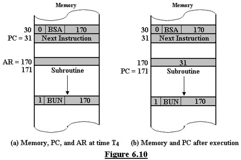
ComputerArchitecture ChapterSix Basic Computer Organization and Design After the fetch and decode phase, PC contains 31, which is the address of the next instruction in the program (the return address). The register AR holds the effective address 170 [see figure 6.10(a)]. The BSA instruction performs the following numerical operation: M[170] 31, PC 170 + 1 =171 The result of this operation is shown in figure 6.10(b). The return address (31) is stored in memory location 170 and control continues with the subroutine program starting from address 171. To accomplished by means of an indirect BUN instruction placed at the end of the subroutine. return to the original program (at address 31), this is When BUN is executed, control goes to the indirect phase to read the effective address at location 170, where it finds the previously saved address 31. Then the effective address 31 is transferred to PC. The next instruction cycle finds PC with the value 31, so control continues to execute the instruction at the return address. ISZ ( Increment and Skip if Zero ) Instruction This instruction increments the word specified by the effective address, and if the result is zero, PC is incremented by one. When PC is incremented by one, the next instruction in the sequence is skipped. The microoperations needed to execute the ISZ instruction are: 25-50 Yacoup K.Hanna
ComputerArchitecture ChapterSix Basic Computer Organization and Design DR M[AR] D6T4: DR DR +1 D6T5: D6T6: M [AR] DR, if (DR = 0) then (PC PC + 1), SC 0 The operation decoder D6 is active when the instruction has an ISZ operation whose binary code value is 110. To execute the ISZ instruction, three timing signals are needed: - 1.The clock transition associated with timing signal T4 read the memory into DR. 2.The clock transition associated with timing signal T5 increments DR. 3.The clock transition associated with timing signal T6 store the word back into memory. In the same clock transition, SC is cleared to 0 which transfers the control to timing signal T0to start a new instruction cycle. 7. Input-Output and Interrupt Computer systems include many types of input and output devices. To demonstrate the most basic requirements for input and output communication, a terminal unit with a keyboard and printer used for this illustration. 1. Input-Output Configuration We mentioned before that the terminals send and receive serial information. Each type of this information has eight bits of an alphanumeric code. The serial information from the keyboard shifted into the input register INPR. The serial information for the printer is stored in the output register OUTR. The two registers INPR & OUTR communicate with an interface serially, and with an accumulator AC in parallel. Figure transmitter interface receives serial information from the keyboard and transmits it to INPR, while the receiver interface receives information from OUTR and sends it serially to the printer. 6.11 shows the input-output configuration. Where the 26-50 Yacoup K.Hanna
ComputerArchitecture Chapter Six Basic Computer Organization and Design The input and output registers INPR & OUTR respectively are 8-bits. They hold alphanumeric information. The input and output flags FGI & FGO are 1-bit control flip-flops. The flag FGI is set to 1 when new information is available in the input device and is cleared to 0 when the information is accepted by the computer. Figure 6.11 Transfer of information from the keyboard to the computer Initially the input flag FGI is cleared to 0. When a key is struck in the keyboard, an 8-bit alphanumeric code is shifted into INPR and the input flag FGI is set to 1. As long as the flag is set, the information in INPR cannot be changed by striking another key. The computer checks the flag bit; if it is 1, the information from INPR is transferred in parallel into AC and FGI is cleared to 0. Once the flag cleared, new information shifted into INPR by striking another key. Transfer of information from the computer to the printer The output register OUTR works similar to INPR, but the direction of information flow reversed. Initially the output flag FGO is set to 1. The computer checks the output flag; if it is 1, the information from AC is transferred in 27-50 Yacoup K.Hanna
ComputerArchitecture Chapter Six Basic Computer Organization and Design parallel to OUTR and FGO is cleared to 0. The output device accepts the coded information, character, and when the operation is completed, it sets FGO to 1. The computer does not load a new character into OUTR when FGO is 0 because this condition indicates that the output device is in the process of printing the character. prints the corresponding 6.7.2. Input-Output Instructions As mentioned before, input-output instructions have an operation code 1111 are recognized by the control ( D7 = 1 & I = 1 ). Bits (0 11) of the instruction specify the particular operation. The control functions and microoperations for the input-output instructions are listed in table 6.5. As shown in the flowchart of figure 6.9, these instructions are executed with the clock transition associated with timing variable T3. Each control function needs the Boolean relation D7I T3, which we designate for convenience by the symbol p. The control function is distinguished by one of the bits in IR (6 -11). By assigning the symbol Bi to bit i of IR, all control functions can be simply denoted by pBifor i = 6 through 11. The sequence counter SC is cleared to 0 when p = D7I T3=1. Table 6.5 Symbol Microoperation SC 0 pB11: AC(0-7) INPR, FGI 0 pB10: OUTR AC(0-7), FGO 0 pB9: if (FGI = 1) then (PC PC + 1) pB8: if (FGO = 1) then (PC PC + 1) pB7: IEN 1 pB6: IEN 0 Description Clear SC Input character Output character Skip on input flag Skip on outputflag Interrupt enable on Interrupt enable off p: INP OUT SKI SKO ION IOF Example The instruction INP has the hexadecimal code F800 (see table 6.2), which gives the binary equivalent 1111 1000 0000 0000. 1. The first bit is one, which indicates I. 2. The next three bits constitute the operation code and are recognized from decoder output D7. 28-50 Yacoup K.Hanna
ComputerArchitecture ChapterSix Basic Computer Organization and Design 3. Bit 11 in IR is 1 and is recognized from B11. Therefore the control function that initiates the microoperation for the instruction INP is D7I T3 B11 = pB11 The execution of input-output instructions completed at time T3 as in the case of the register-reference instructions. The sequence counter SC is cleared to 0 and the control goes back to fetch the next instruction with timing signal T0. The INP instruction transfers the input information from INPR into the eight least significant bits of accumulator and clears the input flag to 0. The OUT instruction transfers the eight least significant bits of accumulator into the output register OUTR and clears the output flag to 0. The instructions SKI & SKO checks the status of the flags FGI & FGO respectively and causes a skip of the next instructions if the flag is 1. The instruction that is skipped will normally be a branch instruction to return and check the flag again. The instructions ION & IOF set and clear an interrupt enable flip-flop IEN. The purpose of the flip-flop IEN will be explained later in conjunction with the interrupt operation. 6.7.3. Program Interrupt The difference of information flow rate between the computer and the input/output device according to the programmed control transfer procedure mentioned before makes this type of transfer inefficient. 29-50 Yacoup K.Hanna
ComputerArchitecture Chapter Six Basic Computer Organization and Design The alternative efficient procedure is to let the external device to inform the computer when it is ready for the transfer. This type of transfer uses the interrupt facility. While the program running, it does not check the input or output flags. However, when a flag is set, the computer shortly interrupted from proceeding with the current program and is informed of the fact that a flag has been set. In that, time the computer deviates shortly from what it is doing to take care of the input or output transfer. After completing the input or output transfer, the computer return to the current program to continue what it was doing before the interrupt. The interrupt flip-flop IEN can be set and cleared according to two instructions as follows: 1. With the IOF instruction, the IEN is cleared to 0 and the input or output flags cannot interrupt the computer. 2. With the ION instruction, the IEN is set to 1, and the computer can be interrupted. How the computer handle the interrupt process The flowchart shown in figure 6.12 explains the process. The computer contains an interrupt flip-flop designated byR. 1. When R = 0, the computer goes through instruction cycle. During the instruction cycle, IEN is checked, if it is 0, indicates no need for interruption, and the control continues with the next instruction cycle. If IEN is 1, control checks the flag bits, if both flags are 0, it indicates that neither the input nor the output registers are ready for transfer of information. In this case, control continues with the next instruction cycle. If either flag is set to 1 while IEN = 1, flip- flop R is set to 1. At the end of execute phase, control checks the value of R, and if it is equal to 1, it goes to an interrupt cycle instead of an instruction cycle. 2. When R = 1, the computer goes through interrupt cycle, which is a hardware implementation of a branch and save return address operation. The return address available in PC is stored in a specific location where it can be found later when the program 30-50 Yacoup K.Hanna
ComputerArchitecture ChapterSix Basic Computer Organization and Design returns to the instruction at which it was interrupted. Here a memory location at address 0 is chosen as the place for storing the return address. Control then inserts address 1 into PC and clears IEN and R so that no more interruptions can occur until the interrupt request from the flag has been serviced. Figure 6.12 Example. (See Figure 6.13) Suppose that an interrupt occurs and R is set to 1 while the control is executing the instruction at address 255. At this time, the return address 256 is in PC. The programmer has previously placed an 31-50 Yacoup K.Hanna
ComputerArchitecture Chapter Six Basic Computer Organization and Design input/output service program in memory starting from address 1120 and BUN 1120 instruction at address 1, see figure 6.13(a). When control reaches timing signal T0and finds that R = 1, it proceeds with the interrupt cycle. The content of PC (256) is stored in memory location 0, PC is set to 1, and R is cleared to 0. At the beginning of the next instruction cycle, the instruction that is read from memory is in address 1 since this is the content of PC. The branch instruction at address 1 causes the program to transfer to the input/output service program at address 1120. This program checks the flags, determines which flag is set, and then transfers the required input or output information. Once this is done, the instruction ION is executed to set IEN to 1 (to enable further interrupts), and the program returns to the location where it was interrupted, see figure 6.13(b). A branch indirect instruction with an address part of 0 placed at the end of the I/O program, returns the computer to the original place in the main program. After this instruction is read from memory during the fetch phase, control goes to the indirect phase (because I = 1) to read the effective address. The effective address is in location 0 and is the return address that was stored there during the previous interrupt cycle. The execution of the indirect BUN instruction results in placing into PC the return address from location 0. 6.7.4. Interrupt Cycle 32-50 Yacoup K.Hanna
ComputerArchitecture Chapter Six Basic Computer Organization and Design From the flowchart shown in figure 6.12, it is clear that the condition for setting flip-flop R to 1 can be expressed with the following register transfer statement: T0T1T2 (IEN )(FGI + FGO): R 1 The interrupt cycle stores the return address which is available in PC into memory location 0, branches to memory location 1, and clears IEN, R, and SC to 0. This can be done with the following sequence of microoperations: AR 0, TR PC M[AR] TR, PC PC +1, RT0 : RT1 : RT2 : PC 0 IEN 0, R 0, SC 0 1.During timing signal T0, AR is cleared to 0, and the contentof PC is transferred to the temporary register TR. 2.During timing signal T1, the return address is stored in memory at location 0 and PC is cleared to 0. 3.During timing signal T3, the PC incremented by 1, clears IEN and R, and control goes back to T0 by clearing SC to 0. The beginning of the next instruction cycle has the condition RT0and the content of PC is equal to 1. The control then goes through an instruction cycle that fetches and executes the BUN instruction in location 1. 6.8. Complete Computer Description 33-50 Yacoup K.Hanna
ComputerArchitecture Chapter Six Basic Computer Organization and Design Figure 6.14 shows the final flowchart of the instruction cycle, including the interrupt cycle for the basic computer. As mentioned before the control returns to timing signal, T0after SC is cleared to 0. if R = 1, the computer execute an interrupt cycle, while for R = 0, the computer executes an instruction cycle. Table 6.6 summarizes the control functions and microoperations for the entire basic computer. Figure6.14 Table 6.6 34-50 Yacoup K.Hanna
ComputerArchitecture ChapterSix Basic Computer Organization and Design Description Fetch Microoperation R'T0: AR PC R'T1: IR M [AR], PC PC+1 R'T2: D0, , D7 Decode IR(12-14), AR IR(0-11), I IR(15) D'7IT3: AR M [AR] Decode Indirect T'0T'1T'2(FGI + FGO): R 1 Interrupt RT0: AR 0, TR PC RT1: M[AR] TR, PC 0 RT2: PC PC+1, IEN 0, R 0, SC 0 D0T4: DR M [AR] D0T5: AC AC DR, SC 0 D1T4: DR M [AR] D1T5: AC AC + DR, E Cout , SC 0 D2T4: DR M [AR] D2T5: AC DR, SC 0 D3T4: M [AR] AC, SC 0 D4T4: PC AR, SC 0 D5T4: M [AR] PC, AR AR +1 D5T5: PC AR, SC 0 D6T4: DR M [AR] D6T5: DR DR +1 D6T6: M [AR] DR, if (DR = 0) then (PC PC + 1), SC 0 r: SC 0 rB11: AC 0 rB10: E 0 rB9: AC AC rB8: E E rB7: AC shr AC, AC(15) E, E AC(0) rB6: AC shl AC, AC(0) E, E AC(15) rB5: AC AC + 1 rB4: If (AC(15) = 0) then (PC PC + 1) rB3: If (AC(15) = 1) then (PC PC + 1) rB2: If (AC = 0) then (PC PC + 1) rB1: If (E = 0) then (PC PC + 1) rB0: S 0 (S is a start-stop flip-flop) p: SC 0 pB11: AC(0-7) INPR, FGI 0 pB10: OUTR AC(0-7), FGO 0 pB9: if (FGI = 1) then (PC PC + 1) pB8: if (FGO = 1) then (PC PC + 1) pB7: IEN 1 pB6: IEN 0 AND ADD LDA Instructions Reference STA BUN BSA Memory ISZ CLA CMA CMA CME CIR CIL INC SPA SNA SZA SZE HLT Instructions Reference Register- INP OUT SKI SKO ION IOF Instructions Output Input / 6.9. Design of the Basic Computer Yacoup K.Hanna 35-50
ComputerArchitecture Chapter Six Basic Computer Organization and Design The hardware of the basic computer consists of the following parts: 1. A memory unit with 4096 words of 16 bits each. 2. Nine registers: AR, PC, DR, AC, IR, TR, OUTR, INPR, and SC. 3. Seven flip-flops: S, E, R, IEN, FGI, FGO, and I. 4. Two decoders: a 3 8 operation decoder and a 4 16 timing decoder. 5. A 16-bit common bus. 6. Control logic gates. 7. Adder and logic circuit connected to the input of AC. The (memory, registers, flip-flops, 3 8 and 4 16 decoders, and the16-bit common bus) have been discussed in details previously in this chapter. These parts can be obtained from a commercial source. Now we are going to design the remaining parts, Control logic gates, and the adder and logic circuit associated with accumulator. 1. Design of the Control logic gates Returning to figure 6.6, which shows some of the inputs to the control logic gates which comes from the two decoders, I flip-flop, and bits 0-11 of IR. Other inputs to control logic gates which are not shown in the figure are: 1. Accumulator 16 bits to check if AC = 0 and to detect the sign bit in AC (15). 2. Data register DR 16 bits to check if DR = 0. 3. Value of the seven flip-flops S, E, R, IEN, FGI, FGO, and I. The outputs of the Control logic circuit are: 1. Signals to control the inputs of the nineregisters. 36-50 Yacoup K.Hanna


![❤Book⚡[PDF]✔ The Apollo Guidance Computer: Architecture and Operation (Springer](/thumb/21611/book-pdf-the-apollo-guidance-computer-architecture-and-operation-springer.jpg)