Understanding Static Timing Analysis in Advanced VLSI Design
Static timing analysis is a crucial aspect of VLSI design, helping predict chip performance before fabrication. This article explores the importance of static timing analysis, its effectiveness, and the limitations of dynamic simulation tools like SPICE. Learn about the challenges in testing critical paths and the difference between static and dynamic analysis in complex circuit designs.

Download Presentation

Please find below an Image/Link to download the presentation.
The content on the website is provided AS IS for your information and personal use only. It may not be sold, licensed, or shared on other websites without obtaining consent from the author. Download presentation by click this link. If you encounter any issues during the download, it is possible that the publisher has removed the file from their server.
E N D
Presentation Transcript
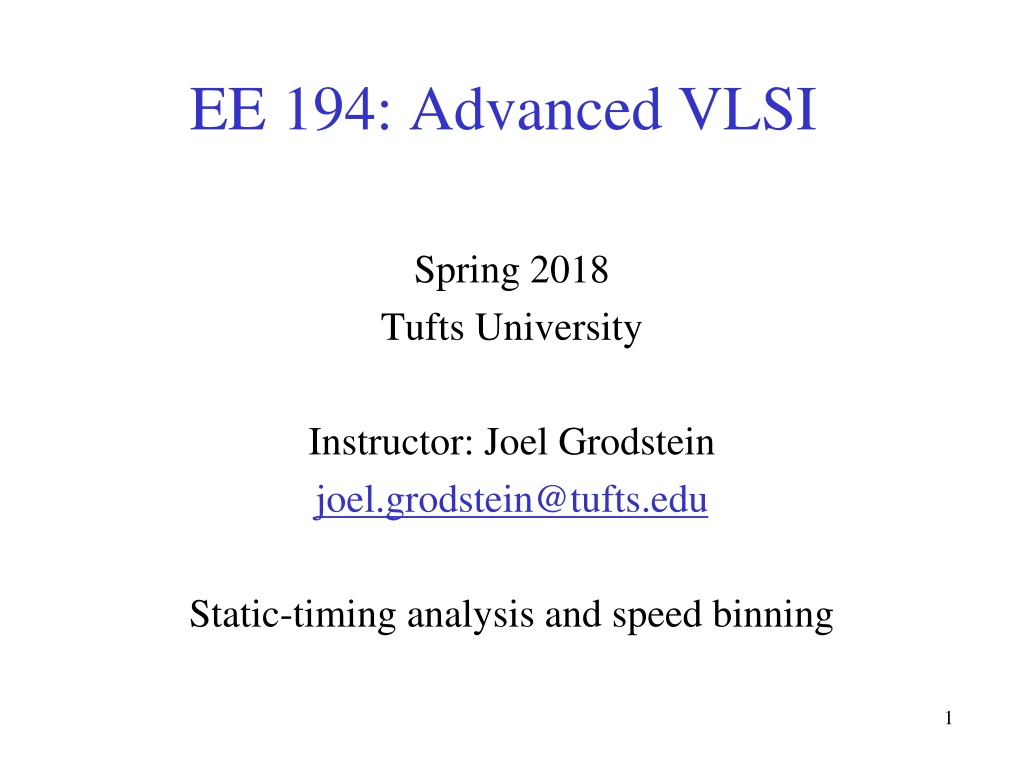
EE 194: Advanced VLSI Spring 2018 Tufts University Instructor: Joel Grodstein joel.grodstein@tufts.edu Static-timing analysis and speed binning 1
Intro What is static-timing analysis? A way to predict how fast our chip will run before we build it. Not bad, huh? Why do we care? Well, we want our chips to run fast, don t we? How well does it work? Pretty well, most of the time So so, some of the time Spectacularly bad, every now and then EE194 Joel Grodstein 2
Cant we just run SPICE? Yes, we could if we didn t mind waiting a few million years . Why so long? The SPICE model is very accurate and so it s slow. But there are reasonably-fast, reasonably-accurate versions of SPICE; that s not really the problem SPICE (or any other simulation) only tests the things that we give it patterns for. EE194 Joel Grodstein 3
Cant we just run SPICE? A AA 1 7 1 D 2 BB B 3 Q 5 0 C Three inputs. Each can rise, fall, stay zero or stay one. How many input patterns for this little network? 43 = 64 It gets real big, real fast, for networks with lots of inputs EE194 Joel Grodstein 4
Cant we just run SPICE? It gets worse Can t we just run SPICE on the important patterns? Who decides what is important? Are you good at thinking, in advance, of every possible issue in a complex design? We want a tool that tests even the critical paths we haven't thought of! EE194 Joel Grodstein 5
Static vs. dynamic Staticusually means pattern-independent, vs. dynamic meaning only for certain input patterns. SPICE is a dynamic simulator; it only simulates the patterns that you give it. Note: it s perfectly fine for modeling our library cells; they just have a few inputs. Can you think of another dynamic simulator commonly used? Most Verilog, VHDL simulators In principle, STA literally checks every path (We'll see later that this is only almost true ) No issues of writing a pattern for a particular path. Sounds great but just how can you check every path? EE194 Joel Grodstein 6
Paths in a toy circuit A AA 7 D 2 BB B 3 Q 5 C What are the paths (from an input to the output)? What are the delays of the 3 paths? red=14, blue=10, green=5. Note the concept: we only trace paths; the logic is irrelevant But will a real circuit have too many paths? EE194 Joel Grodstein 7
Reconvergence A B C 1 1 D 1 1 2 AA 4 BB CC , 2 from B C, 2 from C D 2 paths from A B How many total paths from A to D? 8 paths total, and it's exponential in the depth of the logic. A B C D, A AA B C D, So how can STA check an exponential number of paths? EE194 Joel Grodstein 8
PERT charts Developed by the US Navy in 1950s to manage the Polaris missile project Concerned about the Soviet nuclear arsenal Developed a ballistic missile launched from a submarine Wanted to catch up quickly, hired 3000 contractors, but the resulting schedule mess was too complex They needed an automated method to compute the critical path to developing Polaris. EE194 Joel Grodstein 9
PERT chart for getting to school breakfast (7) 7 lock house (2) 9 dress (3) wake up at t=0 walk to school (5) 3 14 What time do you get to school? What is the critical path? EE194 Joel Grodstein 10
Pert chart for getting to school 0 A breakfast (7) 7 7 lock house (2) 9 2 dress (3) 3 0 B wake up at t=0 walk to school (5) 3 5 14 0 C What works for school, also works for gates. What is the timing & critical path? We have completely ignored the logic function (AND vs. OR, etc) of the network! So the tools to automate a submarine schedule may work for us And in fact STA does work most of the time EE194 Joel Grodstein 11
Pert chart for getting to school A 7 0 7 9 2 0 B 3 3 5 14 0 C Key observations: Again: we have completely ignored the logic function (AND vs. OR, etc) of the network! No need to trace paths from subcritical inputs (this is how we can quickly trace an exponential number of paths) EE194 Joel Grodstein 12
Reconvergence A B C 1 1 D 1 1 2 AA 4 BB CC Figure out the most critical path from A to B. Then totally ignore the A B path! Figure out the most critical way to extend it from B C Then totally ignore any other way to get from B C Ditto from C D No longer tracing an exponential number of paths Assumes the subcritical paths cannot become important If logic mattered, our assumption would be untrue EE194 Joel Grodstein 13
Sequentials Two main types of sequential elements: edge- triggered (usually called flops) and level-sensitive (usually called latches). My drawing convention: D Q CLK D Q CLK latch has a square notch flop has a little triangular notch EE194 Joel Grodstein 14
Flops Q can only change on the rising edge of CLK. The time from when CLK rises to when Q changes is called tclk Q. D is not allowed to change in the red window of tsetup before the rising edge of CLK. Anyone remember why? There s usually an internal state node that could be metastable otherwise CLK D D Q CLK tsetup Q tclk Q EE194 Joel Grodstein 15
Flops and timing Flops are marvelous. No matter what time D changes, it doesn t affect the timing of Q. Q always changes tclk Q after the rising edge of CLK. Let's define t=0 as the rising edge of CLK. Then what is the latest arrival time for Q? If we assign the constant value tclk Q to all flop outputs, then they essentially turn into primary inputs! Thus, STA with loops of flops is very simple. tclk Q CLK D Q tclk Q EE194 Joel Grodstein 16
Flop example (group exercise) AA 8 7 10 C 2 1 BB 4 E 15 OUT 3 5 D Q CLK What is the latest arrival time on the node OUT? (Assume CLK rises at t=0, and tclk Q=1). How about all of the other nodes? What is the fastest cycle time that the circuit can operate at? (Assume tsetup=2). EE194 Joel Grodstein 17 17
What if the clock is nontrivial? B C Q1 3 A D Q 0 1 2 CLK A clock will usually drive long distances and many loads, and will need buffering. Assume CLK rises at t=0, and all gate delays are 1. If tclk Q=1, then what is the arrival time at Q1? So we don t always know our flop-output arrival time up front. How can we deal this this? Just do all of the clocks first. 18 EE194 Joel Grodstein
In-class exercise Assume tclk Q=tsetup=1 4 A 1 D Q 3 Q0 CLK C2 C3 1 1 0 Q1 1 2 B 4 3 D Q 1 What is the arrival time on all nodes? What is the minimum clock cycle time where the circuit functions correctly? Draw the timing diagram on the board, showing both clock R.E. 3 (not 5!) EE194 Joel Grodstein 19
Latches Q can change any time that CLK is high. The time from when D rises to when Q changes is called tD Q, and from CLK rising to Q changing is tclk Q. D is not allowed to change in the red window of tsetup before the falling edge of CLK. CLK D D Q Q CLK tD Q tclk Q EE194 Joel Grodstein 20
Loops of latches D Q D Q C2 C3 CLK All of a sudden, there are two loops. What are they? How can STA figure out the arrival times? It s like a dog chasing its tail First look at the loops. The looping part of any path must be one full cycle. EE194 Joel Grodstein 21
Latches: the summary Latches make STA algorithms more difficult Loop detection and checking is needed Paths flow through latches, and the flow-through path may be critical Algorithms are more complex, but still work fine So why do people use latches? They are more resistant to clock skew But their disadvantages usually outweigh this The homework will explore the issue further. EE194 Joel Grodstein 22
Now the fun begins... So far, as long as we use flops and not latches, static-timing analysis seems easy We ve pulled off the amazing trick of analyzing every path, in just a small amount of time Because of that, we can even check paths we never thought of. Now it s time to take this easy problem and make it hard . OK, really it was hard all along Gate delay, and false paths, and common clocks, oh my Pretty soon you re going to understand why commercial STA tools don t always work perfectly! EE194 Joel Grodstein 23
What does delay mean? We ve talked a lot about delay, but we ve not actually defined it. V Red=inverter input voltage Blue = inverter output voltage Length of black arrow = gate delay How would you define the inverter s delay? Vdd/2 time Interesting question: I drew the black arrow at the point where each waveform crossed Vdd/2. Any thoughts on if this is a good or bad choice? It s probably not the best of choices; it can lead to negative delay! Make sure we know about Vsw EE194 Joel Grodstein 24
What things affect delay? Now we know what delay is... what affects it? Simplest model: the inverter is a resistor, its load (e.g., wiring + downstream gates) is a capacitor. Delay = R*C. Increase R or C, and the output slope gets slower, and the t increases. Vdd R OUT IN inv load C What things affect the values for R and C? Bigger driver devices smaller R; bigger load devices or more wire bigger C. And much more... EE194 Joel Grodstein 25
Input slope Red=input voltage Blue = output voltage Length of black arrow = gate delay V time In reality, the gate delay depends heavily on the slope of the input voltage. Why? Slower input slope means that the output transistors spend less time being fully turned on. We drew our resistor as a fixed resistor depending only on the device size; in reality the resistor size also depends on the input slope. EE194 Joel Grodstein 26
Other things that affect resistance Multiple inputs switching at once When more than one input switches at roughly the same time, it usually affects the gate delay Draw this on the board for a NAND3. What makes it hard to analyze It s often logically impossible for multiple inputs to switch at exactly the same time (but we re not looking at logic) The delay effect is heavily dependent on the exact amount of overlap, so a little bit of analysis error at the inputs means more error at the outputs EE194 Joel Grodstein 27
Capacitive coupling We talked about what affects the R. Now let s talk about the C. V inv1 C1 C2 a grounded capacitor (C1). Bigger C1 slower slew rate on node V, slower delay for inv1, as mentioned. A floating capacitor (C2) is harder. The aggressor (A) can inject charge into the victim (V); the resulting effect on delay varies with the slew rates of V and A, as well as the timing of when they both switch. easily analyze it. inv2 We talked about modeling inv2 and wiring cap as invA A Key idea: model this complex circuit as just an R & C again, so we can EE194 Joel Grodstein 28
Capacitive coupling: case #1 The first case is when the aggressor A is quiet. V inv1 C1 If A does not switch, then A is essentially a ground. The same situation occurs if A does switch, but not at the same time as when V is switching. C2 invA A EE194 Joel Grodstein 29
Capacitive coupling: case #2 A switches in the same direction as V. V inv1 C1 If aggressor A switches at the same time and at the same direction as V, then A and V are always at the same voltage. Then there is no voltage across C2, and no dV/dt, and no charge transfer. It becomes effectively zero. C2 invA A EE194 Joel Grodstein 30
Capacitive coupling: case #3 A switches in the opposite direction as V. V inv1 inv2 C1 If aggressor A switches at the same time and in the opposite direction as V, then the aggressor tries to prevent V from switching. C2 effectively becomes larger (1.5x to 4x, depending on the situation)! C2 kC2 inv3 A EE194 Joel Grodstein 31
The problem with coupling Coupling capacitors arise anytime two wires are near each other. Adjacent metal layers run at 90 to each other, so a long wire has many wires crossing it above and below. There may be thousands of small floating caps attached to a long wire. If we only knew which direction all of those aggressor nodes were switching, and when in the cycle they switched then we could convert them into grounded fixed capacitors and compute the delay for each node, so we could then run timing analysis. But EE194 Joel Grodstein 32
The problem with coupling If we only knew which direction all of those aggressor nodes were switching, and when in the cycle they switched But there are probably many architectural reasons that not all of them can switch the same direction in the same time. Ummm remember we agreed not to let logic functionality enter into STA! But that s what STA is supposed to tell us, and we can t run STA because we don t know gate delays yet! EE194 Joel Grodstein 33
Coupling cap, in practice What do people do in practice? Some caps should be counted at 0x, some at 1x, some at 2x. Compromise: count them all at 1.5x. Or whatever other magic number you chose. And change it if your project is behind schedule . Draw a long-wire example on the board Do full shielding and offset inverters EE194 Joel Grodstein 34
Summary so far False paths, coming up! How well does STA work? Reasonably well, most of the time So so, some of the time Spectacularly bad, every now and then The problems: Capacitive loading greatly affects delay The correct capacitance is essentially impossible to model Multiple-inputs-switching delay variation is also difficult to model correctly EE194 Joel Grodstein 35
What about voltage? How does voltage affect delay? Increase Vdd reduce delay Why? In our model, does it affect R, C or both? Mini-homework: think about it, discuss it with your friends, & we ll discuss it next time EE 194 Joel Grodstein 36
False paths False paths are the bane of STA. We ve made wonderful simplifying assumptions: the problem of timing is completely independent from the logic functionality. Subcritical inputs cannot be part of long paths These are correct 99% of the time but 99% is not nearly good enough! False paths break them . Let s see why. EE194 Joel Grodstein 37
False path with two muxes S The path from B to I is only valid if S=1 The path from I to Q is only valid if S=0 Therefore the path B I Q is a false path. Why would anyone design such a silly circuit? Perhaps it make sense in a larger context. E.g., the first mux is in another faraway block We already use I somewhere in this block. We want Q=mux(S?C:A); we do Q=mux(S?C:I) instead, so as to save a wire. Similar cases occur in a carry-skip adder (see the HW) A 0 I 0 Q B C 1 1 EE194 Joel Grodstein 38
Another mini-homework Can you think of other false-path examples? They re sprinkled throughout computer architecture The BGFs that we ll discuss in the clocking section have them You can look ahead at the HW for the adder example EE 194 Joel Grodstein 39
False path with two muxes 1 S Consider the input arrival times shown above. How should we propagate them? (Assume both muxes have a delay of 1). The green path is false We could ignore the fact that B I Q is false, and claim that the arrival time on Q is 7. However, it really isn t, and this may cause us to mistakenly think the chip doesn t work at speed. The critical path through this logic is A I Q Ugly we ve now intermixed logic & timing. Yes, it s ugly, but there s no choice . Input A is subcritical to the mux but it s the one that matters A 3 0 I 6 0 Q B C 5 2 1 3 or 7? 5 1 EE194 Joel Grodstein 40
How do we know a path is false? Lots of papers in the mid '90s trying to determine this automatically. None was really practical. Where we are today a path is false if somebody says it is. Result: STA is an iterative process 1. Run the STA tool 2. It shows you lots of really long paths that are actually false 3. Tell the tool they are false 4. Go to #1 Question: how much do you trust your architects? EE194 Joel Grodstein 41
Common clocks PLL CLK D Q D Q logic If the clock period is 1000 ps, and the flops have tclk Q=tsetup=0, then how much delay can the logic have? But now let s look at how the clock is actually created. Also 1000ps EE194 Joel Grodstein 42
Real-life problems PLL CLK D Q D Q logic The PLL has jitter. The inverters have unpredictable delay. Why? Delay depends on process, voltage, temperature, coupling capacitors, How long do you think the inverter chain might be for a CPU? Several cycles long! EE194 Joel Grodstein 43
Real-life problems PLL CLK CLKPLL D Q D Q logic Why would we care? No matter how unpredictable or changeable the delay from CLKPLL to CLK, the same CLK feeds both flops. Why would any skew or jitter matter? Clock skew (which is the same every cycle) will not matter here. Clock jitter (which can change every cycle) does. Why? Because the 2nd flop receives a signal a full cycle after the 1st flop sends it i.e., the path starts and ends on different clock edges. EE194 Joel Grodstein 44
The problem with jitter tclk_per CLKPLL t1 t2 CLK Flop #1 output tlogic Flop #2 input Timing constraint: t1+tlogic tclk_per+ t2 or tlogic tclk_per+( t2- t1) And so if t2< t1, we cannot have as much logic. Why would we have t2< t1? Again, changes in voltage, coupling caps. EE194 Joel Grodstein 45
It can get much worse PLL CLK D Q D Q logic Now the common clock is just the first 5 inverters. The final inverter is different for the two flops. How does this make life worse? Unpredictable device size & clock skew can also break our path just like jitter did before Look at the common-clock app (on the class website) EE194 Joel Grodstein 46
Another in-class exercise Assume tclk Q=tsetup=1 Assume the clock buffers each have nominal delay of 1ns .1ns jitter, .2ns skew. A 1 D Q Q0 C4A CLK C2 C3 C4B What is the minimum clock cycle time where the circuit functions correctly? Hint: putting latest arrival times on every gate may not be useful. You may have to look at min/max times on some gates, and may even have to analyze each path separately. Q1 B D Q 1 EE194 Joel Grodstein 47
Another in-class exercise Assume tclk Q=tsetup=1 Assume the clock buffers each have nominal delay of 1ns .1ns jitter, .2ns skew. A 1 D Q 4.3 Q0 2.7-3.3 5.3 C4A CLK C2 .9-1.1 C3 1.8-2.2 C4B Consider the path in blue. Draw the timing diagram. The common clock point is C4A. Do we care about skew? Jitter? Draw the appropriate min/max delay numbers. What is the minimum cycle time? Q1 B D Q 1 Jitter but not skew 5.3+tsetup tc+2.7, or tc 3.6 EE194 Joel Grodstein 48
Another in-class exercise Assume tclk Q=tsetup=1 Assume the clock buffers each have nominal delay of 1ns .1ns jitter, .2ns skew. A 1 D Q 4.5 Q0 3.5 C4A CLK C2 .9-1.1 C3 1.8-2.2 Consider the path in green. Draw the timing diagram. The common clock point is C3. Do we care about skew? Jitter? Jitter but not skew through C3, and both for C4A,C4B 2.5 C4B Q1 B D Q 1 5.5 Draw the appropriate min/max delay numbers. What is the minimum cycle time? 5.5 + tsetup tc+2.5, or tc 4.0 EE194 Joel Grodstein 49
Another in-class exercise What would happen if we had 100 clock buffers instead of just four? The delta between min vs. max would get much bigger, and the minimum clock period would get bigger. CLK A 1 D Q Q0 C4A C2 C3 C4B Q1 Lesson to be learned? Keep jitter low, by keeping di/dt low keeping clock delays fast shielding your clocks B D Q 1 EE194 Joel Grodstein 50


")