Innovations in Pixel Detector Technology for Photon Science
Technologies and advancements in pixel detector development for photon science applications are showcased in this content. Topics discussed include balancing gain and dynamic range in hybrid pixel detectors, performance assessments of integrating pixel detectors, and strategies for photon detection in various experimental setups. The content also explores the utilization of charge sharing for enhanced spatial and energy resolution in pixel detectors, catering to diverse photon science experiments. Overall, these innovations aim to improve imaging capabilities, increase sensitivity for single photon detection, and support high-flux experiments in photon science research.

Download Presentation

Please find below an Image/Link to download the presentation.
The content on the website is provided AS IS for your information and personal use only. It may not be sold, licensed, or shared on other websites without obtaining consent from the author. Download presentation by click this link. If you encounter any issues during the download, it is possible that the publisher has removed the file from their server.
E N D
Presentation Transcript
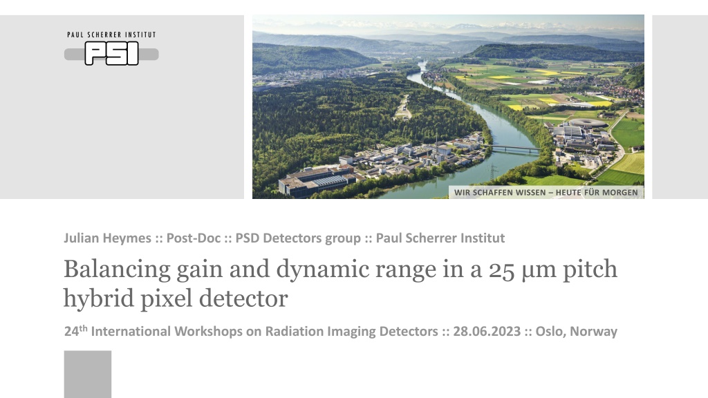
WIR SCHAFFEN WISSEN HEUTE FR MORGEN Julian Heymes :: Post-Doc :: PSD Detectors group :: Paul Scherrer Institut Balancing gain and dynamic range in a 25 m pitch hybrid pixel detector 24thInternational Workshops on Radiation Imaging Detectors :: 28.06.2023 :: Oslo, Norway
The MNCH timeline M NCH0.1 6 Test structures on JUNGFRAU0.1 Technology performance assessment Base design choices 2012 Micropixel with enhanced pOsition rEsolution usiNg CHarge integration JUNGFRAU0.1 M NCH0.2 Full active chip (160 x 160 pixels) 5 pixel architectures (25 m pitch) Area: 4 x 4 mm Charge integrating Small pixel spatial resolution, limited area Analogue readout low noise, lower dark current, high 2012 Technology: UMC 110 nm Standard sensor: 300-320 m thick n-type silicon Typical sensor bias: 200 V Data rate @ 1 kHz/1 cm2: 1.152 TB/hour M NCH0.3 400 x 400 pixels, 25 m pitch 1 cm Implementation of the best M NCH0.2 pixel design (Noise 31 e-RMS) Spatial resolution (interpolated): 1-4 m Also operated with high-Z sensors and LGADs 2014 Today Possible applications using M NCH: (In-vivo) tomography, Resonant Inelastic X-ray Scattering (RIXS), Fourier ptychography, High- resolution imaging, colour imaging, electron microscopy, (Laue diffraction), M NCH0.4 400 x 400 pixels, 25 m pitch 1 cm 19 pixel designs with static and dynamic gain High testability of architectures and components 2018 Today More about detectors for RIXS: Viktoria Hinger s talk (27.06 @ 14:00) 1
A versatile integrating pixel detector for photon science Photon starved experiments with X-ray tubes or at synchrotron beamlines Static gain with low noise for single photon detection (low occupancy 1 %) Fast frame rates (> 1 kHz) with large duty cycles (exposure time frame time) High flux experiments at bright synchrotron beamlines A. B. Static gain with large dynamic range to integrate photons Dynamic gain switching to detect single photons with low noise and integrate larger signals Fast frame rates (> 1 kHz) with large duty cycles (exposure time frame time) Experiments at X-ray Free Electron Lasers Dynamic gain switching to detect single photons with low noise and integrate larger signals Shorter exposure times (~10 s) with readout between bunches (SwissFEL: 100 Hz repetition rate) 2
Using charge sharing Cluster size depends on photon energy, sensor material, sensor bias, sensor thickness Charge sharing Low resolution Analogue High resolution Digital Spatial resolution with interpolation Energy resolution from clustering Charge sharing region in 320 m Si at 120 V 15-20 m Increasing the SNR: low noise and/or hard X-rays Subpixel interpolation with function-based algorithms Examples using Jungfrau with strixels in V. Hinger s presentation Retrieved analogue value in cluster proportional to the detected charge (i.e. photon energy) Preservation of the spectral information Isolated photons required (~1 % occupancy) Fast frame rates and low flux 3
High resolution energy resolved (colour) imaging M NCH0.3 - Siemens Star with spokes 60-0.5 m gold on silicon with silicon microspheres W-anode X-ray tube (40 kV, 200 A) Interpolated to 1 m bins 2x2 cluster spectrum Low flux required for single photon detection Native resolution Full spectrum Native resolution Below Au L-edge Images can be binned in energy Color imaging works also in combination with interpolation. A full spectrum with an energy resolution of about 750 eV FWHM is acquired for each pixel Below the L-edge gold becomes transparent to X-rays Challenges due to polychromatic beam. 4 A Bergamaschi et al., Hybrid Detectors for High Resolution Imaging., Microscopy and Microanalysis, Volume 24, Issue S2, 1 August 2018, Pages 316 319
Application of the interpolation with MNCH0.3 M nch Eiger Jungfrau 2 m gold on 200 m silicon sample fabricated at LXN, PSI Measurement with 10 keV photons at TOMCAT Low flux for single photon detection Native resolution (25 m) 7 m Interpolated to 1 m bins 25 m Also demonstrated with GaAs* More about GaAs at PSI: Kirsty Paton s poster (28.06) 5 *S. Chiriotti, High-spatial resolution measurements with GaAs sensor with the charge integrating M NCH detector , IWoRiD 2021
Benefits of noise reduction Charge sharing Detection level ( Noise) Low resolution Analogue High resolution Digital Low energy detection Reduction of the detection limit: detection of low energy photons even with charge sharing to apply interpolation algorithms Energy resolution from clustering Improvement of the energy resolution Colour imaging 6
MNCH0.4 400 x 400 pixels, 25 m pitch, 1 x 1 cm Designed in UMC110 19 Different pixel variants Analogue readout up to 1.2 kHz 14bit ADC on board (CTB) THR CSA CDS Storage Cells Readout Test structures Overvoltage regulator Dynamic Gain Switching OVERVOLTAGE REGULATOR ResCDS _RES RESET RESET CDS RESET CDS RESET Dsg3 Gain CDS 2 Gain CDS 2 Gain CSA BUSCONNECT _BUSCONNECT ROWSEL READ gHG CCDSg2 Gain CSA CLG CCDSg1 outSFP CHG vdda Gain CDS 1 Gain CDS 1 BUSCONNECT _BUSCONNECT vdda STORE STORE READ READ vIPRECDS CDS CDS CSA CSA 2 3 4 5 1 IN IN Dsg1 CCDSin2 STO0 IN BYPASS CDS CDS BYPASS connCDS CCDSin1 CPULSE vssa PRECHARGE STORAGE STORAGE PRECHARGE bypassCDS PULSE PULSE vIPRE vssa Pulse OFF ENprechPre VprechPre 1 2 3 4 5 STO1 HG / LG vPULSE vssa CSTO1 G1/G2/G4 ROWSEL BYPASS HG / SLG Test structures in pixel SHG / LG STO2 G2/G4/G8 CSTO2 Static gains Alternative readout Debugging architectures SHG No test structure G2/G4/G8 + FILTER Source follower Dynamic Gain Switching 7
Noise results (static gains) highest gains available 19.55 e- 31.01 e- 30.64 e- 20.69 e- 18.07 e- 1 1 s exposure time 1 kHz readout rate 5 3 4 2 1 2 3 4 5 HG / LG G1/G2/G4 Test structures in pixel HG / SLG SHG / LG G2/G4/G8 No test structure SHG G2/G4/G8 + FILTER 8
Spectral response to Fe fluorescence (2x2 clusters) 1 2 3 4 5 LGAD REGION 1 2 3 4 5 HG / LG G1/G2/G4 Test structures in pixel HG / SLG SHG / LG G2/G4/G8 No test structure SHG G2/G4/G8 + FILTER More about LGADs: Jiaguo Zhang s poster (28.06) Per pixel calibration of M NCH: Erik Fr jdh s poster (26.06) 9
Linearity (Energy calibration with 2x2 clusters) Gain difference between SHG and SHG min due to parasitics 1 2 3 4 5 1 2 3 4 5 HG / LG G1/G2/G4 Test structures in pixel HG / SLG SHG / LG G2/G4/G8 No test structure SHG G2/G4/G8 + FILTER 10
Dynamic range (static gains) Larger errors at high signals due to non-linearities (under investigation) 1 Measurement method Dynamic range 1) Red laser focused in one pixel of an etched device 2) Intensity modulated by pulsing the laser N times (N=[0;100], period=100 ns) during the exposure (10 s) 3) ND filter applied to tune saturation before maximum number of pulses 4) Signal in central pixel converted to charge from X-ray calibration data Gain 11
Balance of noise and dynamic range (static gains) Noise [e-] / Dynamic range [12 keV photons] 2 LG-G1 LG-G2 LG-G4 HG-G1 HG-G2 HG-G4 1 3 4 5 1 2 M03VM04 176/78 175/41 164/21 70/16 50/9.2 34/5.2 LG185BigNcap 181/162 184/100 212/69 70/17 52/10 37/5.5 LG-G2 LG-G4 LG-G8 SHG-G2 SHG-G4 SHG-G8 3 SHG 174/39.5 158/27 125/12.5 35.5/6.5 30/4 21.6/2.2 SHG-G2 SHG-G4 SHG-G8 SHG-G2 SHG-G4 SHG-G8 4 5 SHG min 32.6/6 28.6/3.5 20.5/2 32.8/6 28/3.2 20.1/1.9 SHG min filt 30.5/6.3 26.18/3.7 19.3/2.1 30.5/6.2 25.1/3.7 18.9/2.1 Low Gain 1 2 3 4 5 HG / LG G1/G2/G4 Test structures in pixel HG / SLG SHG / LG G2/G4/G8 No test structure SHG G2/G4/G8 + FILTER 12
DGS architectures overview (for high-intensity applications) OVERVOLTAGE REGULATOR PSI WEST THR SLS PSI EAST RESET CDS RESET Gain CDS 2 Gain CSA Gain CDS 1 STORE READ CSA CDS IN BYPASS CDS PRECHARGE STORAGE PULSE Main requirements At FELs: Shorter exposure times (~10 s) with readout between bunches (SwissFEL: 100 Hz repetition rate) At Synchrotrons: Fast frame rates (> 1 kHz) with large duty cycles (exposure time frame time) Must handle very large signals from several (hundreds of) photons impinging during exposure while maintaining single photon resolution Dynamic gain switching + overvoltage protection Challenges with DGS in small pixels Very limited area (1/9thJUNGFRAU) Only two preamp gains available (3 in JUNGFRAU), no burst mode Current must be reduced to a minimum while keeping speed for efficient DGS Architecture with higher noise, but needs to be kept under control 13
DGS in 25 m pixel, it works - (DGS 3 G1) Scan of intensity by changing ND filters Single pixel. Average of 100 frames DAC value = Threshold Dynamic gain switching implemented in the 25 m pitch. Architectures inherently noisier than with static gain Baseline of both gains well aligned. CDS gain limited to G1 for larger DR at HG without saturation Low gain noise after switching equivalent to noise with low gain forced (around 480 e-, for all CDS gains) Cross-talk at lower thresholds and from other architectures (e.g. shared biases) 14
The future of MNCH M NCH0.5, a short term intermediate prototype Design starting end of 2023 for an early 2024 MPW run Image area: 4 x 4 mm2, 160 x 160 pixels (M NCH0.2 format) Implementation of an optimised pixel design, and improvements from Jungfrau s developments Pixel validation with in-lab characterisations and pilot experiments at beamlines 1-side butted M NCH1.0 2.56 x 3.84 cm2 M NCH1.0, a full-scale small pixel pitch HPD Planned submission in 2025 and single chip module in 2026 Image area: Up to 3 x 2 cm2(single chip). Example: 2.56 x 1.92 cm2 (1024 x 768 pixels) Implementation of on-chip ADCs and DACs + improvements from other developments M NCH1.0 2.56 x 1.92 cm2 Open questions: Implementation of Dynamic Gain Switching? N-sides buttability? (Example of a 1-side buttable sensor) Sensors M0.3/M0.4 1 x 1 cm2 Open challenges: Power distribution over a large area + power consumption (high density + readout rate) Massive data rates and volumes. For 1024 x 768 pixels: - At 1 kHz: 1.58 GB/s (5.67 TB/hour) - At 10 kHz: 15.8 GB/s (57.6 TB/hour) Software for on-line data processing (+ AI ?) Hits and clusters extraction See Xiangyu Xie s talk about deep-learning for EM (28.06 @ 09:00) M0.2/M0.5 4 x 4 mm2 15
Thank you for your attention Contact: julian.heymes@psi.ch PSD Detectors group Back: Jiaguo Zhang, Aldo Mozzanica, Thomas King, Davide Mezza, Anna Bergamaschi, Julian Heymes Middle: Erik Fr jdh, Carlos Lopez, Martin Br ckner, Christian Ruder, Bernd Schmitt, Konstantinos Moustakas, Dominic Greiffenberg Front: Viktoria Hinger, Dhanya Thattil, Roberto Dinapoli, Shqipe Hasanaj, Maria Carulla, Simon Ebner Missing: Rebecca Barten, Pawel Kozlowski, Filippo Baruffaldi, Xiangyu Xie, Kirsty Paton V. Hinger and K. A. Paton have received funding from MSCA PSI-FELLOW-III-3i (EU grant agreement No. 884104) 16
Backup 17
High resolution imaging: in-situ mouse lung tomography M NCH0.3 - 22 keV @ SYRMEP, Elettra (Trieste, Italy) Direct conversion: lower dose for similar image quality as with CCDs or CMOS (with converters) 25 m pitch good enough for imaging with direct conversion Christian Dullin et al., J. Synchrotron Rad. (2018). 25, 565 569 18
Application of the interpolation with MNCH03 M nch Eiger Jungfrau 2 m gold on 200 m silicon sample fabricated at LMN Measurement with 10 keV photons at TOMCAT Native resolution (25 m) 7 m Interpolated to 1 m bins 5 m bins (GaAs:Cr) Interpolated to 25 m S. Chiriotti, High-spatial resolution measurements with GaAs sensor with the charge integrating M NCH detector , IWoRiD 2021 19
Noise r.m.s. results highest gain available 19.55 e- 70.8 eV 31.01 e- 112.3 eV 30.64 e- 110.9 eV 20.69 e- 74.9 eV 18.07 e- 65.4 eV SHG min M NCH03 LG185 SHG min filter SHG 1 s exposure time 1 kHz readout rate 20


 imaging")


 – highest gains available")
")
")
")
")
")