Understanding Sequential Circuits and Flip-Flops
Explore the concept of sequential circuits and flip-flops in digital systems. Learn how memory elements and feedback play a crucial role in constructing these circuits, essential for storing information. Discover the difference types of shift registers and counters built with flip-flops, including NAND latches as fundamental building blocks.

Download Presentation

Please find below an Image/Link to download the presentation.
The content on the website is provided AS IS for your information and personal use only. It may not be sold, licensed, or shared on other websites without obtaining consent from the author. If you encounter any issues during the download, it is possible that the publisher has removed the file from their server.
You are allowed to download the files provided on this website for personal or commercial use, subject to the condition that they are used lawfully. All files are the property of their respective owners.
The content on the website is provided AS IS for your information and personal use only. It may not be sold, licensed, or shared on other websites without obtaining consent from the author.
E N D
Presentation Transcript
SEQUENTIAL CIRCUITS Dr.S.Vaaheedha Kfatheen Assistant Professor Department of Computer Science & IT Jamal Mohamed College (A) Trichy 620 020. 2
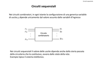
FLIP FLOPS - In a sequence circuit the output at any point of time depend not only o the present inputs. But also on the previous input sequence. - Sequential circuits are characterized by memory and a feedback between the outputs and inputs. - A sequence circuit is constructed from combinational circuit, with a feedback path between the output and input. 3
Inputs Outputs Memory elements Combinational circuit Definition A flip flop is a Bi-stable device (that is) it can remain in one of the two stable state which are designated as 0 and 1 state. 4
- It is the fundamental logic circuit used for storing information in digital systems. - Difference types of shift registers and counters are design only using flip flops, which can be built using NOR gates or NAND gates. - A flip flops has two outputs, one of which is the complement of the other. - They are called normal (Q) output and complementary (Q ) output. 5
A NAND LATCH - NAND latch or NOR latch is the fundamental built in block in constructing a flip flop. - It has the property of holding on to any previous output, as long as it is not disturbed. 6
- A latch has 2 outputs Q and Q - When the circuit is switched ON the latch may enter into any state. - If Q=1, then Q =0 which is called SET state - If Q =0, then Q=1, which is called RESET state - Whether the latch is in SET state or RESET state it will continue to remain in the same state as long as the power is not switched OFF. 8
- The latch is not an useful circuit since there is no way of entering the desired input. - It is the fundamental building block in constructing the flip flop. 9
1. RS FLIP FLOP - RS flip flop is constructed with 4 NAND gates it has two inputs S and R & two outputs Q & Q . Block Diagram R Q S Q RS FLIP FLOP 10
INPUT OUTPUT S R 0 0 0 1 1 0 1 1 Q(n+1) 0 0 1 1 MODE HOLD RESET SET PROHIBITED 12
- The working of the RS flip flop is as follows: CASE 1: When S=0 and R=0 both the NAND gates A and B output is 1. - Hence the outputs of C & D depend only on the feedback inputs - The entire circuit behaves as a latch - The circuit will hold on to its previous output - This state is called Hold State. 13
CASE 2: - When S=0 and R=1 NAND gate A output will be 1 and B output is 0. - The output of D (that is ) Q will be 1, making both inputs to get C as 1. - Hence Q will be in 0 state. This state of flip flop is known as RESET state. 14
CASE 3: - When S=1 and R=0, then Q=0 and Q=1 - This state of the flip flop is known as SET state. CASE 4: - When S=1 and R=1, this input condition is prohibited because when both Q & Q =1. - This is against the principle of operation of a flip flop. 15
- Moreover if the inputs are now change, the next state of the flip flop is unpredictable. - The next state actually depends on which gate faster to change its present state. - This prohibited state is also called as RACE condition. 16
CLOCKED RS FLIP FLOP - A clock is a timing signal, generate by a master clock generator in a digital system. - These timing signals are distributed through out the digital system. - The clock waveform is a square waveform. - The clock signal synchronous various functional units. - It determines when a system should have an input and generate an output. 17
- When a clock signal applied at the input of a gate, it is enable only when the clock is 1. - When the clock is 1, the other inputs to the gate are accepted by the gate. - When the clock is 0, the inputs are not accepted by the gate. 18
Block Diagram R Q S Q Clock RS FLIP FLOP 19
Characteristic Table INPUTS Clk S 0 X 1 0 1 0 1 1 1 1 Q(n+1) Q(n) Q(n) 0 1 * OUTPUTS R X 0 1 0 1 MODE HOLD HOLD RESET SET RACE 21
- It has 3 inputs, S,R and Clk - It has 2 outputs Q and Q - The operation of the RS flip flop is as follows. - If there is no signal at the clock input, the output of the circuit cannot change irrespective of the values at input S & R. - Only when the clock signals change from 0 to 1 the output will be affected according to the values in input S & R. 22
- If S=1 and R=0 output Q is SET to 1. - If S=0 and R=1 output Q is cleared to 0. - If both S and R =0 the output does not change. - When both S and R=1 the output is unpredictable. - This state is referred to as forbidden state. - The x on the table show that when clock=0, whatever may be the values of S & R the circuit does not respond. 23
D FLIP FLOP Block Diagram D Q Q Clock D FLIP FLOP 24
CLK 0 1 1 D X 0 1 Q(n+1) Q(n) 0 1 MODE HOLD RESET SET 26
- An SR flip flop is converted to a D flip flop by inserting an inverter between S & R and assigning the symbol D to the single input. - The D input is sampled during the occurrence of a clock transition from 0 to 1. - If D=1, the output of the flip flop goes to the one state. - If D=0, the output of the flip flop goes to the zero state. - D flip flop is also called as transparent latch 27
J K FLIP FLOP - The prohibited or RACE condition of the RS flip flop is eliminated by modifying it into a JK flip flop. - In this flip flop the output Q and Q of an flip flop are feed back to the RS inputs using two AND gates must be inputs. 28
J K FLIP FLOP Block Diagram J Q K Q Clock RS FLIP FLOP 29
Characteristic Table INPUTS Clk J 0 X 1 0 1 0 1 1 1 1 Q(n+1) Q(n) Q(n) 0 1 Q(n) OUTPUTS K X 0 1 0 1 MODE HOLD HOLD RESET SET TOGGLE 31
- The circuit diagram and characteristic table of the JK flip flop shows that it has 3 inputs J,K and clock and it has 2 outputs Q and Q. - If there is no signal and the clock input the output of the circuit cannot change irrespective of values at J and K. - When the clock signal=1, the J and K inputs are processed. - If J=1 and K=0 output is SET to 1. - If J=0 and K=1 output is cleared to 0. - When J=1 and K=1 a clock transition switches the outputs of the flip flop to their complement state. 32
T FLIP FLOP Block Diagram T Q Q Clock T FLIP FLOP 33
CLK 0 1 1 T X 0 1 Q(n+1) Q(n) Q(n) Q (n) MODE HOLD HOLD TOGGLE 35
- It has two inputs T and clock. - This T flip flop is obtained from a J & K flip flop when inputs J and K are connected to provide a single input designated by T. - The T flip flop has only two conditions when T=0 the clock transition does not change the state of the flip flop. - When T=1, a clock transition complements the state of the flip flop. 36
- In a JK flip flop, if it is clocked, a situation called RACE condition will occur. - This happens when the inputs J&K are equal to 1 and the clock period is much larger than the propagation delay of the gates. - Under this situation when the new outputs RACE around to the inputs. They find the clock to be still high and hence cause the outputs toggle again. 38
- This repeats as long as the clock is high and the final output when the clock becomes low is unpredictable. - This problem can be eliminated by using a Master-Slave flip flop. - A Master-Slave flip flop consists of 2 cascaded JK flip flop - The clock to 1 flip flop, master is inverted and applied to the other flip flop, slave. - Hence, whenever master is active and the slave is inactive and vice versa. 39
- The master will accept the JK inputs when the clock makes a positive transition and the slave will copy the master s output at its output when the clock makes a negative transition. - It is to be noted that the final output appears only when the clock is low. - When J=1 and K=0- The master flip flop is SET to 1 during the positive clock pulse and the slave is SET during the following negative clock pulse. 40
When J=0 and K=1 - The master flip flop is RESET to 0 during the positive clock pulse and the slave is RESET during the following negative clock pulse. - When J=1 and K=1 - The master flip flop toggles during the positive clock pulse and the slave toggles during the following negative clock pulse. 41
COUNTERS - A counter is a sequential logic circuit that counts the number of incoming clock pluses. - A register that goes through a pre-determined sequence of state upon the application of input pulses. USES - Counts the number of incoming clock pluses. - Generating timing signal to control the sequence of operation in digital computers. 42
- Basically there are two types of counters. - 1. Synchronous - 2. Asynchronous Asynchronous counters or serial counter The ripple counter is simple and straight forward in operation. Construction requires a minimum of hardwires. It have a speed limitation. Each flip flop is triggered by the previous flip flop. 43
Synchronous or parallel counter - An increase in speed of operation can be achieved by use of a parallel counter. - Every flip flop is triggered by the clock - Serial and parallel counters are used in combination to compromises between speed of operation and hardware count 44
Asynchronous counters(Ripple counters) - A binary ripple counter can be constructed by use of clocked JK flip flop. 45
3 bit binary ripple counter J A J A J A Clock K A K A K A C A B 46
Truth Table CLOCK TRANSITION C B A 0 0 0 0 1 0 0 1 2 0 1 0 3 0 1 1 4 1 0 0 5 1 0 1 6 1 1 0 7 1 1 1 0 0 0 0 47
- The system clock (a square wave) derives flip flop A - The output of A derives B and the output of B derives flip flop C - All the J and K inputs are tied to +Vcc. This means that each flip flop will change state with a Ve transition at its clock input. - The flip flop must change states before it can triggered the B flip flop and the B flip flop has to change states before it can trigger the c flip flop. 48
- The triggers move through the flip flops ripple in water. - A act as the clock for B, each time the wave form at A goes low, flip flop B will toggle. - Since B act as the clock for C each time the waveform at B goes low flip flop C will Toggle. 49
Synchronous counters - Ripple counter is the simplest counter to build - But there is a limit to its highest operating frequency. - In ripple counter each flip flop has a delay time - Total setting time for the counter is approximately the delay time. Times the total number of flip flops. - These problems can be overcome by the use of a synchronous or parallel counter. - In synchronous counter every flip flop is triggered in synchronization with the clock. 50


")


 derives flip flop")