Understanding Fundamental Concepts of Interrupts in Embedded Systems
Explore the fundamental concepts of interrupts in embedded systems, including interrupt handling, maskability, priority, service routines, and interrupt vectors. Learn how interrupts allow the CPU to handle special events efficiently, coordinate I/O activities, and prevent CPU tie-up, enhancing system performance and reliability.

Download Presentation

Please find below an Image/Link to download the presentation.
The content on the website is provided AS IS for your information and personal use only. It may not be sold, licensed, or shared on other websites without obtaining consent from the author. Download presentation by click this link. If you encounter any issues during the download, it is possible that the publisher has removed the file from their server.
E N D
Presentation Transcript
INTERRUPTS AND RESETS Razvan Bogdan Embedded Systems
Content Fundamental Concepts of Interrupts HCS12 Exceptions Interrupt programming in C Language Clock and Reset Generation Block Computer Operating Properly Low-Power Modes Stop Mode, Resets HCS12 Operation Modes
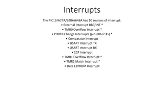
Fundamental Concepts of Interrupts What is an interrupt? A special event that requires the CPU to stop normal program execution and perform some service related to the event Examples of interrupts include I/O completion, timer time-out; illegal opcodes, arithmetic overflow, divide-by-0, underflow (software interrupts, also known as traps, exceptions) Functions of Interrupts Coordinating I/O activities and preventing CPU from being tied up Providing a graceful way to exit from errors Reminding the CPU to perform routine tasks
Fundamental Concepts of Interrupts Interrupt Maskability Interrupts that can be ignored by the CPU are called maskable interrupts. A maskable interrupt must be enabled before it can interrupt the CPU. An interrupt is enabled by setting an enable flag. Interrupts that can t be ignored by the CPU are called non- maskable interrupts.
Fundamental Concepts of Interrupts Interrupt priority Allow multiple pending interrupt requests Resolve the order of service for multiple pending interrupts Interrupt Service CPU executes a program called the interrupt service routine A complete interrupt service cycle includes 1. Saving the program counter value in the stack 2. Saving the CPU status (including the CPU status register and some other registers) in the stack 3. Identifying the cause of interrupt 4. Resolving the starting address of the corresponding interrupt service routine 5. Executing the interrupt service routine 6. Restoring the CPU status and the program counter from the stack 7. Restarting the interrupted program
Fundamental Concepts of Interrupts Interrupt Vector Starting address of the interrupt service routine; Interrupt Vector Table A table where all interrupt vectors are stored. Methods of Determining Interrupt Vectors Predefined locations (Microchip PIC18, 8051 variants) Fetching the vector from a predefined memory location (HCS12, Atmel avr) Executing an interrupt acknowledge cycle to fetch a vector number in order to locate the interrupt vector (68000 and x86 families) 1. 2. 3.
Fundamental Concepts of Interrupts Steps of Interrupt Programming how to provide service to the interrupt Step 1. Initializing the interrupt vector table Step 2. Writing the interrupt service routine: A service routine is similar to a subroutine the only difference is the last instruction. An interrupt service routine uses the return-from- interrupt (or return-from-exception) instruction instead of return- from-subroutine instruction to return to the interrupted program Step 3. Enabling the interrupt: an interrupt can be enabled by clearing the global interrupt mask and setting the local interrupt enable bit in the I/O control register Don t forget to enable interrupts when writing the code
Fundamental Concepts of Interrupts The Overhead of Interrupts Saving and restoring of CPU status and other registers. (HCS12 needs to save all CPU registers). Execution time of instructions of the interrupt service routine. The execution of the RTI instruction that will restore all the CPU registers. Exercise: try to calculate it Resets The initial values of some CPU registers, flip-flops, and the control registers in I/O interface chips must be established in order for the computer to function properly. The reset mechanism establishes these initial conditions for the computer system. There are at least two types of resets: power-on reset and manual reset. The power-on reset establishes the initial values of registers and I/O control registers. The manual reset without power-down allows the computer to get out of most error conditions if hardware doesn t fail. A reset is non-maskable.
HCS12 Exceptions Maskable interrupts: including IRQ pin and all peripheral function interrupts. Nonmaskable interrupts: including XIRQ pin, SWI interrupt, and unimplemented opcode trap. Resets: including the power-on reset, RESET pin manual reset, the COP reset (computer operate properly), and clock monitor reset. For other microcontrollers, the COP reset is also called the watchdog reset.
HCS12 Exceptions. Maskable interrupts Different HCS12 members implement different number and types of peripheral functions, and hence may have different number of maskable interrupts. One of the maskable interrupts can be raised to the highest priority among the maskable interrupt group and receive quicker service. This is achieved by programming the HPRIO register.
HCS12 Exceptions. Maskable interrupts The priority and vector addresses of all HCS12 exceptions are listed in Table 6.1. To raise a maskable interrupt source to the highest priority, write the low byte of the vector address of this interrupt to the HPRIO register. For example, to raise the capture timer channel 6 interrupt to the highest priority, write the value of $E2 to the HPRIO register. In Table 6.1, exceptions that have higher vector addresses are at higher priorities. Not all the exceptions are available in all HCS12 members. IRQ Pin Interrupt The only external maskable interrupt for the HCS12. IRQ interrupt can be edge-triggered or level-triggered. IRQ interrupt has a local enable mask in the IRQCR register. The IRQ interrupt is configured by programming the IRQCR register. The contents of the IRQCR register are shown in Figure 6.2.
HCS12 Exceptions. Maskable interrupts
HCS12 Exceptions. Maskable interrupts Making IRQ Level-Sensitive (active low): Whenever one of the interrupt sources (that are tied to the IRQ pin) is low, an interrupt request will be detected by the HCS12 Pros: Multiple interrupt sources can be tied to this pin. Cons: Need to make sure that the IRQ signal has become inactive before the IRQ service routine is complete if there is only one interrupt request pending. Making IRQ Edge-Sensitive (falling edge) Pros: No need to control the duration of the IRQ pulse. Cons: Not suitable for noisy environment because every falling edge caused by noise will be recognized as an interrupt. When does the MCU recognize interrupt requests? The MCU recognizes the interrupt request when it completes the execution of the current instruction unless the current instruction is a fuzzy logic instruction. For fuzzy logic instructions, the HCS12 recognizes the interrupt immediately.
HCS12 Exceptions. Maskable interrupts The Stack Order on Entry of an Interrupt The HCS12 saves all CPU registers on an interrupt. The order of saving CPU registers is shown in the figure The RTI Instruction RTI is used to terminate interrupt service routines. RTI will restore CPU registers from the stack. The HCS12 will continue to execute the interrupted program unless there is another pending interrupt.
HCS12 Exceptions. Nonmaskable interrupts Non-maskable Interrupts There are three interrupts in this category: XIRQ pin, SWI instruction, & unimplemented instruction opcode trap. XIRQ Pin Interrupt XIRQ interrupt is disabled during a system reset and upon entering the service routine of another XIRQ interrupt. After minimal system initialization, software can clear the X bit of the CCR register to enable the (using the andcc #$BF instruction) XIRQ interrupt. Software cannot reset the X bit once it has been set. When a non-maskable interrupt is recognized, both the X and I bits are set after CPU registers are saved. The execution of an RTI instruction at the end of the XIRQ service routine will restore the X and I bits to the pre-interrupt request state.
HCS12 Exceptions. Nonmaskable interrupts Unimplemented Opcode Trap There are 202 unimplemented opcode (16-bit opcode). These unimplemented opcode share the same vector $FFF8:$FFF9. Software Interrupt Instruction (SWI) Execution of the SWI instruction causes an interrupt without an interrupt request signal. The SWI instruction is commonly used in the debug monitor to implement breakpoints and to transfer control from a user program to the debug monitor. A breakpoint in a user program is a memory location where we want program execution to be stopped and information about instruction execution (in the form of register contents) to be displayed.
Interrupt programming in C Language CodeWarrior Template for Interrupt Service Routine Interrupt void ISR_name (void) { // statements to service the interrupt } There are two parts in setting up the interrupt service routine: 1. Declare the interrupt service to be external 2. Insert the name of interrupt service routine into the appropriate place of the interrupt vector table For example, IRQ interrupt vector can be setup as follows:
Interrupt programming in C Language external void near irqISR(void); // IRQ pin is defined outside this file #pragma CODE_SEG_NEAR_SEG NON_BANKED // interrupt section for this module _interrupt void UnimplementedISR(void) { for(;;); // do nothing, but return from interrupt } #pragma CODE_SEG DEFAULT typedef void (*near tIsrFunc)(void); const tIsrFunc _vect[] @0xFF80 = {// interrupt vector table starts from this line // interrupt vector table UnimplementedISR, irqISR, // IRQ interrupt vector (at the address 0xFFF2) }; The entry UnimplementedISR is provided as a catch-all handler for all unintended interrupts.
Interrupt programming in C Language Interrupt Programming in EGNU IDE 1. Use the interrupt attribute of the GCC compiler. Add the following statements at the beginning of the program: #define INTERRUPT __attribute__((interrupt)) 2. Apply the interrupt attribute to the interrupt service routine. void INTERRUPT irqISR(void); 3. Include the header file vectors12.h to your program : #include c:\egnu\include\vectors12.h 4. Store the name of the IRQ service routine at the designated address: UserIRQ = (unsigned short)&IRQISR; 5. Write the actual IRQ service routine.
Interrupt programming in C Language Example 1: The IRQ pin of the HCS12DP256 is connected to a 1-Hz digital waveform and port B is connected to eight LEDs. Write a program to configure port B for output and enable the IRQ interrupt and also write the service routine for the IRQ interrupt. The service routine for the IRQ interrupt simply increments a counter and outputs it to port B. C language version of the program is to be compiled by GNU C compiler. Solution: #include "c:\egnu\include\hcs12.h" #include "c:\egnu\include\vectors12.h" #define INTERRUPT __attribute__((interrupt)) void INTERRUPT IRQISR(void); unsigned char cnt; void INTERRUPTIRQISR(void) { cnt++; PTB = cnt; } void main(void) { UserIRQ = (unsigned short)&IRQISR; DDRB = 0xFF; cnt = 0; DDRJ |= BIT1; PTJ &= ~BIT1; IRQCR = 0xC0; asm("cli"); while(1); } // configure PJ1 pin for output // enable LEDs to light // enable IRQ interrupt on falling edge // enable interrupt globally // wait for interrupt forever
Clock and Reset Generation Block (CRG) CRG generates the clock signals required by the HCS12 instruction execution and all peripheral operations. The clock signal has the form of square waveform. Crystal oscillators are often used to generate clock signals. The crystal oscillator output is a sinusoidal wave and must be converted to square wave before it can be used. The HCS12 has internal circuit to do this square up operation. The CRG block also has a PLL circuit that can multiply the frequency of the incoming clock signal. The CRG can also accept oscillator output (square waveform) directly. The XCLKS signal must be tied low (for MC9S12DP256B) in order to use external clock signal.
CRG Configuration Registers: MC9S12DP256B Device User Guide
Choice of clock Source This circuit generates the system and core clocks used in the microcontroller. When dealing with external memory or peripheral modules, the bus clock (E-clock) is used. The E-clock is derived by dividing the SYSCLK clock by 2. If the PLLCLK is chosen to be the SYSCLK, then the frequency of the E-clock is half that of PLLCLK. Either the oscillator output OSCCLK (when PLLSEL = 0) or the PLL output PLLCLK (PLLSEL = 1) can be selected as SYSCLK. The oscillator can be completely bypassed and turned off by selecting an external clock source instead. The clock monitor, PLL, RTI, COP, and all clock signals based on OSCCLK are driven by this external clock instead of the output of the oscillator.
Choice of clock Source The user can choose between using the external crystal or oscillator to produce the clock signal. The external crystal is connected between the EXTAL and XTAL pins and needs an on-chip oscillator circuitry to square it up. The external clock source provided by the oscillator is connected to the EXTAL pin and has a 2.5V peak to peak magnitude for D family (9s12DP256)
Phase Locked Loops The PLL circuit has the capability to multiply incoming signal frequency and stabilize its output signal frequency. The frequency of the PLLCLK is controlled by registers SYNR and REFDY using the following equation: PLLCLK = 2 OSCCLK (SYNR + 1) (REFDV + 1) (6.1) NOTE: PLLCLK must not exceed the maximum operating system frequency; maximum bus frequency is 25 MHz. => maximum PLLCLK is 50 MHz.
Phase Locked Loops Selection of PLL for clock generation is controlled by the CRGSEL register. 7 6 5 4 3 2 1 0 SYSWAI ROAWAI PLLWAI CWAI RTIWAI COPWAI PLLSEL PSTP 0 0 reset: 0 0 0 0 0 0 PLLSEL: PLL select bit 0 = system clocks are derived from OSCCLK 1 = system clocks are derived from PLLCLK PSTP: pseudo stop bit This bit controls the functionality of the oscillator during the stop mode. 0 = oscillator is disabled in stop mode 1 = oscillator continues to run in stop mode (pseudo mode). The oscillator amplitude is reduced. SYSWAI: system clocks stop in wait mode bit 0 = The system clocks continue to run in wait mode. 1 = The system clocks stop. ROAWAI: Reduced oscillator amplitude in wait mode bit 0 = Normal oscillator amplitude in wait mode 1 = Reduced oscillator amplitude in wait mode PLLWAI: PLL stops in wait mode bit 0 = PLL keeps running in wait mode 1 = PLL stops in wait mode. The CRG will clear the PLLSEL bit before entering wait mode. The PLLON bit remains set during wait mode but the PLL is powered down. CWAI: core stops in wait mode bit 0 = Core clock keeps running in wait mode. 1 = Core clock stops in wait mode. RTIWAI: RTI stops in wait mode bit 0 = RTI keeps running in wait mode. 1 = RTI stops and initializes the RTI dividers whenever the part goes into wait mode. COPWAI: COP stops in wait mode bit 0 = COP keeps running in wait mode 1 = COP stops and initializes the COP dividers whenever the part goes into wait mode. Figure 6.13 The CRG clock select register (CRGSEL)
Phase Locked Loops PLL is also controlled by the PLLCTL register. 7 6 5 4 3 2 1 0 ACQ 0 PRE SCME CME PLLON AUTO PCE 0 0 reset: 0 0 0 0 0 0 CME: clock monitor enable bit 0 = clock monitor is disabled 1 = clock monitor is enabled. Slow or stopped clocks will cause a clock monitor reset sequence or self clock mode PLLON: phase lock loop on bit 0 = PLL is turned off 1 = PLL is turned on. If AUTO bit is set, the PLL will lock automatically. AUTO: automatic bandwidth control bit 0 = automatic mode control is disabled and the PLL is under software control, using ACQ bit. 1 = high bandwidth filter is selected ACQ: acquisition bit (if AUTO bit = 1, this bit has no effect) 0 = low bandwidth filter is selected 1 = high bandwidth filter is selected PRE: RTI enable during pseudo stop bit 0 = RTI stops running during pseudo stop mode 1 = RTI continues running during pseudo stop mode PCE: COP enable during pseudo stop bit 0 = COP stops running during pseudo stop mode 1 = COP continues running during pseudo stop mode. SCME: self clock mode enable bit 0 = detection of crystal clock failure causes clock monitor reset 1 = detection of crystal clock failure forces the MCU in self clock mode Figure 6.14 The CRG PLL control register (PLLCTL)
Phase Locked Loops Example 2: There is a system that derives its bus clock (E-clock) from the PLL circuit and an external clock of 8 MHz is selected. The desired bus clock is 24 MHz. Write an assembly routine and a C function to perform the configuration. Solution: - Since the E-clock frequency is higher than the external clock s, we need to use the PLL circuit - The SYSCLK frequency is 48 MHz - The frequency of OSCCLK is 8 MHz The XCLKS pin must be grounded to select oscillator as clock source! 48 MHz = 2 X 8 MHz X [SYNR + 1] /[REFDV + 1] One solution is to set SYNR and REFDV to 2 and 0, respectively. SetClk8 movb #02,SYNR #0,REFDV #$80,CLKSEL #$60,PLLCTL CRGFLG,LOCK,* ; set SYNR to 2 ; set REFDV to 0 ; enable PLL, keep SYSCLK running in wait mode, ; keep RTI, COP, PLL & core running in wait mode ; disable clock monitor, enable PLL, set automatic ; bandwidth control, disable RTI & COP in pseudo stop ; wait until PLL locks into the target frequency movb movb movb brclr rts
Phase Locked Loops Example 2 (cntd.): There is a system that derives its bus clock (E-clock) from the PLL circuit and an external clock of 8 MHz is selected. The desired bus clock is 24 MHz. Write an assembly routine and a C function to perform the configuration. Solution: - Since the E-clock frequency is higher than the external clock s, we need to use the PLL circuit - The SYSCLK frequency is 48 MHz - The frequency of OSCCLK is 8 MHz The XCLKS pin must be grounded to select oscillator as clock source! 48 MHz = 2 X 8 MHz X [SYNR + 1] /[REFDV + 1] One solution is to set SYNR and REFDV to 2 and 0, respectively. void SetClk8(void) { SYNR = 0x02; // use PLL and 8-MHz crystal to generate 24-MHz E clock REFDV = 0; // CLKSEL = 0x80; //enable PLL, keep SYSCLK running in wait mode PLLCTL = 0x60; // enable PLL, set automatic bandwidth control while(!(CRGFLG & 0x08); // wait until PLL locks into the target frequency }
Phase Locked Loops Example 3: There is a system that uses a 4 MHz crystal oscillator to derive a 24 MHz bus clock (E-clock). Write an instruction sequence to perform the required configuration. Solution: - The SYSCLK frequency is 48 MHz - The frequency of OSCCLK is 4 MHz The XCLKS pin must be pulled to high to select external crystal to generate clock signals !!! 48 MHz = 2 X 8 MHz X [SYNR + 1] /[REFDV + 1] One solution is to set SYNR and REFDV to 5 and 0, respectively. SetClk4: rts movb #05,SYNR ; set SYNR to 5 movb #00,REFDV ; set REFDV to 0 movb #$80,CLKSEL ; enable PLL, keep SYSCLK running in wait mode, ; keep RTI, COP, PLL & core running in wait mode movb #$60,PLLCTL ; disable clock monitor, enable PLL, set automatic ; bandwidth control, disable RTI & COP in pseudo stop ClkWait: brclr CRGFLG,LOCK ,ClkWait ; wait until PLL locks
Clock Monitor The clock monitor circuit is based on an internal resistor-capacitor (RC) time delay so that it can operate without any MCU clocks. If no OSCCLK edges are detected within this RC time delay, the clock monitor indicates failure which asserts self clock mode or generates a system reset depending on the state of SCME bit. If the clock monitor is disabled or the presence of clocks is detected no failure is indicated. The clock monitor function is enabled/disabled by the CME control bit. (PLLCTL) If no OSCCLK edges are detected within the RC time delay, the clock monitor may reset the MCU if the CME bit in the PLLCTL register is set to 1. The SCME bit of the PLLCTL register must be cleared to 0 for clock monitor to work.
Real-Time Interrupt The RTI can be used to generate a hardware interrupt at a fixed periodic rate. If enabled (by setting RTIE=1), this interrupt will occur at the rate selected by the RTICTL ($003B) register. At the end of the RTI time-out period the RTIF flag is set to 1 and a new RTI time-out period starts immediately. A write to the RTICTL register restarts the RTI time-out period. If the PRE bit is set, the RTI will continue to run in Pseudo-Stop Mode (in PLLCTL) The RTI interrupt is enabled by the interrupt enable register (CRGINT). Problem: How to construct the interrupts periods?
Real-Time Interrupt 7 6 5 4 3 2 1 0 0 LOCKIE 0 0 RTIE 0 0 SCMIE 0 0 reset: 0 0 0 0 0 0 RTIE: real time interrupt enable bit 0 = interrupt requests from RTI are disabled. 1 = interrupt requests from RTI are enabled. LOCKIE: lock interrupt enable bit 0 = LOCK interrupt requests are disabled. 1 = LOCK interrupt requests are enabled. SCMIE: self clock mode interrupt enable bit 0 = SCM interrupt requests are disabled 1 = Interrupt will be requested whenever the SCMIF bit is set Figure 6.11 The CRG interrupt enable register (CRGINT) 5 7 6 2 1 4 3 0 RTR0 0 RTR5 RTR4 RTR3 RTR2 RTR1 RTR6 reset: 0 1 0 0 0 0 0 0 Figure 6.16 CRG RTI control register (RTICTL)
Real-Time Interrupt Analysis: Seven bits (RTR6-0) in the RTICTL register specify the interrupt rate. The 7-bit value is composed of two parts: Let RTR6, RTR5, RTR4 be n, which is a 3-bit number ranging from 0 to 7 Let RTR3, RTR2, RTR1, RTR0 be m, which is a 4-bit number ranging from 0 to 15 Remember that 3 registers are to be used with RTI: If n is 0 then RTI is off
Real-Time Interrupt A 9S12C32 with an 8 MHz crystal will have an OSCCLK frequency of 8 MHz and a default E-clock frequency of 4 MHz. A 9S12DP512 with a 16 MHz crystal will have an OSCCLK frequency of 16 MHz and a default E-clock frequency of 8 MHz. Let fcrystal be the crystal frequency, then the RTI interrupt frequency can be calculated using => The interrupt rate is determined by the crystal clock and the RTICTL value
Real-Time Interrupt 9S12 real-time interrupt period in ms, assuming an 8 MHz crystal:
Real-Time Interrupt 9S12 real-time interrupt period in ms, assuming an 16 MHz crystal:
Real-Time Interrupt Exercise 4: Write a software that increments a global variable every 32.768 ms. Solution: The solution will use a periodic RTI interrupt that occurs every 32.768 ms. RTI is simple, and accurate if the desired interrupt period matches one of the possibilities shown in the previous value tables. The main program executes RTI_Init to initialize the RTI interrupts. The RTI rate is determined by the crystal frequency and the RTICTL register. Bit 7 of the CRGINT register is set to arm the RTI system. The RTI_Init routine initializes the global variable and enables interrupts (cli). The ISR will acknowledge the interrupt and increment a global variable, Time. The ISR makes the trigger flag zero by writing a one to it
Real-Time Interrupt Exercise 4 (cntd.): Write software that increments a global variable every 32.768 ms. Solution: Exercise: Write software that increments a global variable every 16.38 ms, 16 MHz crystal.
Real-Time Interrupt Exercise 5: Write a C program to use the RTI interrupt to time-multiplex four seven segment displays using the circuit shown below and shift the seven-segment display pattern as described. Turn on one display at a time and light each display for about 1 ms then switch to the next display. Use display #0 to display #5. Use CodeWarrior and a demo board programmed with serial monitor to implement the circuit. 123456 234567 345678 456789 567890 678901 789012 890123 901234 012345
Real-Time Interrupt Exercise (cntd.) - Solution: Arangement: Place the segment patterns in one array segPat[]. Place digit select values in the array digit[]. Use the variable seq as index to the segment array that identifies the first digit of the current sequence. Use the variable ix as an index to the digits within one sequence (ix = 0..5). Use the variable count to specify the repetition count of a sequence #include "c:\cwHCS12\include\hcs12.h" #include "c:\cwHCS12\include\SetClk.h" int seq; int ix; int count; char segPat[13] = {0x06,0x5B,0x4F,0x66,0x6D,0x7D,0x07,0x7F,0x67,0x3F,0x06, 0x5B,0x4F}; char digit[6] = {0xFE,0xFD,0xFB,0xF7,0x7F,0xBF}; // start index to segPat[] of a sequence of digits (0 to 9) // index of digits of a sequence (0 to 5) // repetition count of a sequence
Real-Time Interrupt Exercise (cntd.) - Solution: void main (void) { seq = 0; ix = 0; count = 400; SetClk8(); RTICTL = 0x40; DDRB = 0xFF; DDRP = 0xFF; CRGINT|= RTIE; asm("CLI"); while(1); } // RTI interrupt service routine interrupt void rtiISR(void) { CRGFLG = 0x80; PTB = segPat[seq+ix]; // send out digit segment pattern PTP = digit[ix]; // turn on the display ix++; // increment the index to digits of a sequence if (ix == 6) // make sure the index to digits of a sequence is from 0 to 5 ix = 0; count--; if(count == 0){ // is time for the current sequence expired? seq++; count = 400; } if(seq == 10) // is this the last sequence? seq = 0; } This project also contains the vectors.c file. // initialize the start index to segPat[] for the display sequence // initialize the index of a new sequence // initialize the RTI interrupt count of a sequence // set E clock to 24 MHz from an 8-MHz crystal oscillator // RTI interrupt interval set to 1 msec // configure Port B for output // configure Port P for output // enable RTI interrupt // enable interrupt globally // clear RTIF bit // // change to a new sequence of digits // reset repetition count // reset start index of a sequence
Real-Time Interrupt Exercise 5 (cntd.) - Solution: Arangement: extern void near rtiISR(void); #pragma CODE_SEG __NEAR_SEG NON_BANKED #pragma CODE_SEG DEFAULT // Change code section to DEFAULT. typedef void (*near tIsrFunc)(void); const tIsrFunc _vect[] @0xFFF0 = { rtiISR };
Computer Operating Properly (COP) COP is a free running watchdog timer that allows the user to determine whether the user program is running and sequencing properly. The COP is a timer circuit that will time out if it is not rearmed within a preset time limit. The COP will reset the MCU when it times out and the user would know if the software operated properly. The time out period of the COP is controlled by the COPCTL register. The application software must include an instruction sequence to prevent the COP from timing out when this is enabled. To prevent the COP from timing out for applications that uses COP function, write $55 and then $AA into the ARMCOP register.
Computer Operating Properly (COP) 7 6 5 4 2 1 3 0 WCOP RSBCK CR2 CR1 CR0 0 0 0 reset: 0 1 0 0 0 0 0 0 WCOP: windowed COP mode bit When set, a write to the ARMCOP register must occur in the last 25% of the selected period. A write during the first 75% of the selected period will reset the MCU. 0 = normal COP operation 1 = windowed COP operation RSBCK: COP and RTI stop in active BDM mode bit 0 = allows the COP and RTI to keep running in active BDM mode 1 = stops the COP and RTI whenever the HCS12 is in active BDM mode CR2:CR0: COP watchdog time rate select (number of OSCCLK cycles) 000: COP disabled 001: 214 010: 216 011: 218 100: 220 101: 222 110: 223 111: 224 Figure 6.17 CRG COP control register (COPCTL)


")
")


")
")