Two-Stage Op-Amp Design for GBW and Phase Margin


Two-stage op-amp: design for
GBW
and Phase Margin
P. Bruschi – Design of Mixed Signal Circuits
1

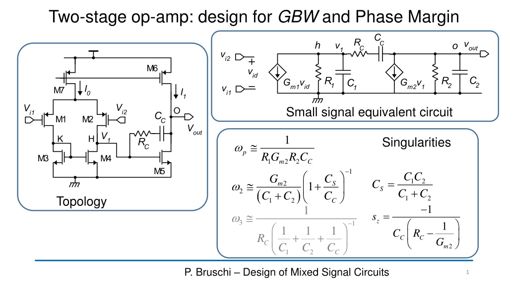
Topology
Small signal equivalent circuit


Singularities


Preliminary assumptions
P. Bruschi –Design of Mixed Signal Circuits
2
In this design procedure, we
decide to cancel the zero:
We consider that the
GBW
and phase margin can be estimated by
using a two-pole approximation of the frequency response, with a
dominant pole (
p
):
P. Bruschi – Design of Mixed Signal Circuits
3
GBW and unity-gain angular frequency (
0
)
GBW and stability specifications
P. Bruschi – Design of Mixed Signal Circuits
4
Then, we impose:
An approximate approach: Hypothesis 1
P. Bruschi – Design of Mixed Signal Circuits
5
Hypothesis 1:
C
1
is much smaller than
C
2
and
C
C
:
Motivation:
C
2
includes the load capacitance,
C
L
C
C
can be made arbitrarily large to satisfy
the hypothesis
An approximate approach: Hypothesis 2
P. Bruschi – Design of Mixed Signal Circuits
6
Hypothesis 2: The parasitic component
C
2
' is much smaller than
C
L
:
Now the expression of
2
is
strongly simplified
Hypotheses 1 and 2 correspond
to consider that all parasitic
capacitances of the amplifier are
negligible with respect to
C
L
and
C
C
, which are external to the
amplifier (
C
L
) or are purposely
placed devices (
C
C
).
The
GBW
specification shapes the second stage (
G
m
2
)
P. Bruschi –Design of Mixed Signal Circuits
7
For the stability requirement:
stability
specification
GBW specification
Back to the first stage
P. Bruschi – Design of Mixed Signal Circuits
8
We have two degrees of freedom, G
m1
and C
C
: a smaller G
m1
would allow for a smaller C
C
value, saving area. However, C
C
cannot get too small, otherwise hypothesis 1 risks to fail.
To guide the choice, it is convenient to relate
C
C
to
C
L
and to the
G
m
1
/
G
m
2
ratio, through the stability condition
stability condition
C
C
and
C
L
, the "rule of thumb" and its limits
P. Bruschi –Design of Mixed Signal Circuits
9
If we make
C
C
=
C
L
, validity of condition (a) makes also condition (b)
automatically true. Making
C
C
even larger than
C
L
does not add
validity to hypothesis 1 and requires more area.
Hypothesis 1
Rule of thumb:
We have determined
both
G
m1
and
G
m2
(a)
(b)
Limits of the rule of thumb
P. Bruschi – Design of Mixed Signal Circuits
10
C
a
s
e
o
f
l
a
r
g
e
C
L
:
I
f
t
h
e
m
a
x
i
m
u
m
l
o
a
d
c
a
p
a
c
i
t
a
n
c
e
i
s
p
a
r
t
i
c
u
l
a
r
l
y
l
a
r
g
e
(
>
t
e
n
s
p
F
)
,
u
s
i
n
g
t
h
e
r
u
l
e
o
f
t
h
u
m
b
c
a
n
r
e
s
u
l
t
i
n
t
o
o
l
a
r
g
e
a
c
o
m
p
e
n
s
a
t
i
o
n
c
a
p
a
c
i
t
a
n
c
e
,
a
n
d
t
h
e
n
,
i
n
n
o
n
-
a
c
c
e
p
t
a
b
l
e
c
h
i
p
a
r
e
a
o
c
c
u
p
a
t
i
o
n
.
I
n
t
h
o
s
e
c
a
s
e
s
,
t
h
e
C
C
/
C
L
c
a
n
b
e
m
a
d
e
s
m
a
l
l
e
r
t
h
a
n
o
n
e
(
C
C
<
C
L
)
i
n
o
r
d
e
r
t
o
m
a
k
e
C
C
e
a
s
i
l
y
i
n
t
e
g
r
a
b
l
e
.
Rule of thumb:
Often, it is convenient to apply a different
choice
For example: with
C
L
=100 pF,
I choose:
C
C
=10 pF
P. Bruschi –Design of Mixed Signal Circuits
11
Application of the design procedure to our simple two-stage op-amp
Once the M1 and M5
overdrive voltages have
been chosen, the
GBW
specification determines
the aspect ratios (
W
/
L
)
of both MOSFETs
in strong inversion
GBW
and supply current
P. Bruschi – Design of Mixed Signal Circuits
12
P. Bruschi – Design of Mixed Signal Circuits
13
GBW
,
C
L
and supply current
•
The higher the
GBW and load capacitance
C
L
,
the higher the supply current and then
the power consumption
•
For the same
GBW
and
C
L
specifications,
lower supply currents can be obtained
with the lowest
V
TE
5
and
V
TE
1
.
Robustness against
C
L
variations
P. Bruschi – Design of Mixed Signal Circuits
14
I
f
w
e
r
e
d
u
c
e
C
L
,
t
h
e
n
C
2
r
e
d
u
c
e
s
a
n
d
h
y
p
o
t
h
e
s
i
s
1
m
a
y
b
e
n
o
m
o
r
e
v
a
l
i
d
.
T
h
e
n
w
e
h
a
v
e
t
o
u
s
e
t
h
e
c
o
m
p
l
e
t
e
e
x
p
r
e
s
s
i
o
n
f
o
r
2
:
gets smaller
gets smaller
Effects of
C
2
reduction:
Both denominators reduces
2
increases!
We have designed
the op-amp for the
maximum
C
L
. It must
be stable also for
smaller values
P. Bruschi – Design of Mixed Signal Circuits
15
Robustness against
C
L
variations
C
L
decreases:
greater phase
margin
C
L
increases:
smaller phase
margin
In a two-stage amplifier:
•
Reducing
(or even removing) the load capacitance
improves
stability
•
Increasing the load capacitance reduces stability and eventually causes
instability
Is nearly unaffected by
C
L
Limits of the simplified design procedure
P. Bruschi – Design of Mixed Signal Circuits
16
Given a
GBW
specification, the procedure can be summarized in the
following way
1. Find the required G
m2
value from the equation:
2. Choose a proper C
C
/C
L
ratio, depending on the value of C
L
3. Find the required G
m1
:
It seems that using the required current to set
G
m2
and
G
m1
to the correct value,
we can reach an arbitrarily high GBW, independently of the process being
used. This is clearly not reasonable.
Limits of the simplified design procedure
P. Bruschi – Design of Mixed Signal Circuits
17
The problem stands in the hypotheses the procedure is based on.
The hypotheses derive from the fact that
C
L
is generally prevalent over
the parasitic capacitances:
Trying to get larger and larger
G
m
2
and
G
m
1
increases also the size of the
MOSFETs in the first and second stage, causing violation of the hypotheses
can be satisfied choosing a large enough
C
C
.
Hyp. 1
Hyp. 2
Limits of the simplified design procedure
P. Bruschi – Design of Mixed Signal Circuits
18
I can still set C
C
as large as to
make C
S
/C
C
<<1
P. Bruschi – Design of Mixed Signal Circuits
19
Limits of the simplified design procedure
P. Bruschi – Design of Mixed Signal Circuits
20
GBW
In this region
the hypotheses
are valid
Maximum achievable
GBW
Increasing
g
m5
for a given
f
T5
,
increases
C
gs5
proportionally
L
5
(V
GS
-V
t
)
5
In strong inversion
GBW tends to
saturate to f
T5
/
The slew rate problem
P. Bruschi – Design of Mixed Signal Circuits
21
v
id
Just after a step variation of the
input voltage, the feedback
voltage, derived by the output
voltage, cannot change
instantaneously and the input
differential voltage of the op-
amp can be driven out of the
linearity region of the first stage
If the input step is large enough, the
input stage saturates
Slew rate in Miller-compensated two-stage op-amps
P. Bruschi – Design of Mixed Signal Circuits
22
The second stage can be represented
as an inverting amplifier with gain
G
m
2
R
2
.
Impedance
Z
L
represents the load
condition. If
Z
L
has a resistive
component, the gain of the second
stage will be smaller than
G
m
2
R
2
.
Z
L
includes the load capacitance
P. Bruschi – Design of Mixed Signal Circuits
23
Slew rate in Miller-compensated two-stage op-amps
(
I
o
1-
max
can be either
negative or positive)
Note that current
I
F
flows also through the output terminal of the
amplifier. Then, the analysis shown above is applicable if the second
stage (output stage) is capable of producing the total current
I
F
+
I
L
If the gain of the second stage is high
enough, we can consider virtual gnd at
input v
1
.
Slew rate of the simple class-A, two stage op-amp.
P. Bruschi – Design of Mixed Signal Circuits
24
From simple inspection of the first stage:
For a given
GBW
, the higher
V
TE1
, the
higher the slew rate
Singularities in the small-signal equivalent circuit are analyzed for the two-stage op-amp design aiming for a specific GBW and phase margin. The preliminary assumptions involve canceling a zero and approximating the frequency response with dominant poles. Specifications for stability, unity-gain angular frequency, and stability requirements are discussed. Hypotheses are proposed to simplify component considerations, and the second stage is shaped to meet stability specifications.

Download Presentation

Please find below an Image/Link to download the presentation.
The content on the website is provided AS IS for your information and personal use only. It may not be sold, licensed, or shared on other websites without obtaining consent from the author.If you encounter any issues during the download, it is possible that the publisher has removed the file from their server.
You are allowed to download the files provided on this website for personal or commercial use, subject to the condition that they are used lawfully. All files are the property of their respective owners.
The content on the website is provided AS IS for your information and personal use only. It may not be sold, licensed, or shared on other websites without obtaining consent from the author.
E N D
Presentation Transcript
Two-stage op-amp: design for GBW and Phase Margin Small signal equivalent circuit 1 Singularities p RG R C 1 2 2 m C 1 C C C 1 G C C = C 1 + 2 + 1 2 C m S ( ) S C 2 + C Topology 1 2 1 1 2 C = s z 3 1 1 1 C 1 1 C R + + R C C G C C C 2 m 1 2 C P. Bruschi Design of Mixed Signal Circuits 1
Preliminary assumptions 1 1 = s = In this design procedure, we decide to cancel the zero: R z 1 C G C R 2 m C C G 2 m We consider that the GBW and phase margin can be estimated by using a two-pole approximation of the frequency response, with a dominant pole ( p): 3, , 2 2 p tail mirror P. Bruschi Design of Mixed Signal Circuits 2
GBW and unity-gain angular frequency (0) = = 2 f f GBW A f 0 0 p 0 0 = 2 A f = A 0 0 p 0 0 p 1 p RG R C 1 2 2 m C A G RG R 0 1 1 2 2 m m G RG R RG R C G C = 1 1 2 2 1 m m m 0 1 2 2 m C C P. Bruschi Design of Mixed Signal Circuits 3
GBW and stability specifications G C = 0 GBW 1 m 0 2 C f f = = 70 3 2 m 0 = Then, we impose: 2 0 1 G C C + 1 2 C m S ( ) 2 + C 1 2 C P. Bruschi Design of Mixed Signal Circuits 4
An approximate approach: Hypothesis 1 C C C C Hypothesis 1: C1is much smaller than C2and CC: Motivation: C2includes the load capacitance, CL CCcan be made arbitrarily large to satisfy the hypothesis 2 1 1 C C C C 1 S C 1 G C G C C G 2 m = + 1 2 C 2 C m S m ( ) ( ) 2 2 + + C C 2 1 2 1 2 C P. Bruschi Design of Mixed Signal Circuits 5
An approximate approach: Hypothesis 2 Hypothesis 2: The parasitic component C2' is much smaller than CL: G C G C Now the expression of 2is strongly simplified = + 2 2 2' m m C C C C 2 2 L L 2 L Hypotheses 1 and 2 correspond to consider that all parasitic capacitances of the amplifier are negligible with respect to CLand CC, which are external to the amplifier (CL) or are purposely placed devices (CC). P. Bruschi Design of Mixed Signal Circuits 6
The GBW specification shapes the second stage (Gm2) stability specification G C 2 m = For the stability requirement: 2 = 2 2 0 L GBW 2 f 2 0 2 GBW G C GBW 2 2 m GBW specification 2 G GBW C 2 m L L P. Bruschi Design of Mixed Signal Circuits 7
Back to the first stage 2 G GBW C 2 m L 1 = R C G 2 m We have two degrees of freedom, Gm1and CC: a smaller Gm1 would allow for a smaller CCvalue, saving area. However, CC cannot get too small, otherwise hypothesis 1 risks to fail. To guide the choice, it is convenient to relate CCto CL and to the Gm1/Gm2ratio, through the stability condition G C 1 m 0 C 1 G G C C G C G C stability condition = = = 1 m C 2 1 m m 2 0 2 m L L C P. Bruschi Design of Mixed Signal Circuits 8
CCand CL, the "rule of thumb" and its limits 1 G G C C (a) C C C C = 1 2 1 m C L C Hypothesis 1 (b) 2 m L 1 C If we make CC=CL, validity of condition (a) makes also condition (b) automatically true. Making CCeven larger than CLdoes not add validity to hypothesis 1 and requires more area. 1 = C C = Rule of thumb: G G With =3 (?? 70 ) C L 1 2 m m 1 3 We have determined both Gm1and Gm2 = G G 1 2 m m P. Bruschi Design of Mixed Signal Circuits 9
Limits of the rule of thumb Often, it is convenient to apply a different choice = C C Rule of thumb: C L Case of large CL: If the maximum load capacitance is particularly large (> tens pF), using the rule of thumb can result in too large a compensation capacitance, and then, in non-acceptable chip area occupation. In those cases, the CC/CLcan be made smaller than one (CC<CL) in order to make CCeasily integrable. For example: with CL=100 pF, I choose: CC=10 pF 1 1 1 30 G G C C = = 1 m C 10 2 m L P. Bruschi Design of Mixed Signal Circuits 10
Application of the design procedure to our simple two-stage op-amp = 2 G g GBW C C C 2 5 m m L 1 1 C C = = = C C G g G g 1 1 2 5 m m m m L L Once the M1 and M5 overdrive voltages have been chosen, the GBW specification determines the aspect ratios (W/L) of both MOSFETs in strong inversion g W L W L W L W L = = 1 m 1 g C V V 1 1 m p OX GS t C V g V 1 1 p OX GS t 1 1 ( ) = = 5 5 m 5 g C V V ( ) 5 m n OX GS t C V V 5 5 n OX GS t 5 5 P. Bruschi Design of Mixed Signal Circuits 11
GBW and supply current = + 2 I I I 1 5 supply D D I = = g I m TE g V D m D V TE = + 2 I g V g V 1 1 5 5 supply m TE m TE g g = + 2 1 m I g V V 5 5 1 supply m TE TE 5 m g g = + 2 2 2 1 g GBW C m I GBW C V V 5 5 1 m L supply L TE TE 5 m P. Bruschi Design of Mixed Signal Circuits 12
GBW, CLand supply current g g = + 2 2 1 m I GBW C V V 5 1 supply L TE TE 5 m 1 g g G G C C = = 1 1 m m C 5 2 m m L The higher the GBW and load capacitance CL, the higher the supply current and then the power consumption For the same GBW and CLspecifications, lower supply currents can be obtained with the lowest VTE5and VTE1. P. Bruschi Design of Mixed Signal Circuits 13
Robustness against CLvariations We have designed the op-amp for the maximum CL. It must be stable also for smaller values + 2' C C L If we reduce CL, then C2reduces and hypothesis 1 may be no more valid. Then we have to use the complete expression for 2: Effects of C2reduction: 1 1 C 1 1 G = + C gets smaller = 2 C m ( ) S C 2 C C + C 2increases! + 1 2 1 S 1 2 C C gets smaller S C C Both denominators reduces P. Bruschi Design of Mixed Signal Circuits 14
Robustness against CLvariations CLincreases: smaller phase margin CLdecreases: greater phase margin arctan 2 m 0 1 G G C = 2 C m Is nearly unaffected by CL 1 m ( ) 2 C C + C 0 + 1 S 1 2 C C In a two-stage amplifier: Reducing (or even removing) the load capacitance improves stability Increasing the load capacitance reduces stability and eventually causes instability P. Bruschi Design of Mixed Signal Circuits 15
Limits of the simplified design procedure Given a GBW specification, the procedure can be summarized in the following way G C GBW = 2 2 m 1. Find the required Gm2value from the equation: 2 L 2. Choose a proper CC/CLratio, depending on the value of CL 1 C C 3. Find the required Gm1: = C G G 1 2 m m L It seems that using the required current to set Gm2and Gm1to the correct value, we can reach an arbitrarily high GBW, independently of the process being used. This is clearly not reasonable. P. Bruschi Design of Mixed Signal Circuits 16
Limits of the simplified design procedure The problem stands in the hypotheses the procedure is based on. The hypotheses derive from the fact that CLis generally prevalent over the parasitic capacitances: = + C C C C , ' 2' C C C C C C C Hyp. 2 2 1 1 2 2 L L L Hyp. 1 can be satisfied choosing a large enough CC. 1 C Trying to get larger and larger Gm2and Gm1increases also the size of the MOSFETs in the first and second stage, causing violation of the hypotheses P. Bruschi Design of Mixed Signal Circuits 17
Limits of the simplified design procedure = GBW 2 2 f 2 0 1 G 1 = = 2 C m GBW ( ) 2 C C + 2 C I can still set CC as large as to make CS/CC<<1 2 + 1 S 1 2 C G 2 C m ( ) 2 + C 1 2 1 G C 1 G = = 2 ' m 2 C m GBW ( ) ( ) + + + 2 C C 2 C 1 2 L 1 2 P. Bruschi Design of Mixed Signal Circuits 18
Limits of the simplified design procedure 1 G C = 2 ' m GBW ( ) + + 2 C C 1 2 L = + + C C C C C 1 5 ' 2 4 5 GS DB DB GS = + C C C C 2 5 6 5 DB DB GS 1 g 5 m + GBW ( ) 2 C C 5 GS L 1 1 g 5 m GBW 1 f 5 T GBW 2 C C + 5 GS 1 L C 1 g + 1 L C 5 m f 5 GS C 5 T 2 C 5 GS 5 GS P. Bruschi Design of Mixed Signal Circuits 19
Maximum achievable GBW g 1 g C = 5 m C 5 m C C 5 gs 2 f 5 gs L 2 5 T L 1 f 5 T GBW Increasing gm5for a given fT5, increases Cgs5proportionally C Tf + 1 L C C 5 5 gs L C 5 GS C C 5 gs L GBW In strong inversion In this region the hypotheses are valid 1 2 Tf L5 (VGS-Vt)5 5 GBW max g C GBW tends to saturate to fT5/ = 5 m GBW C C 3 1 L 5 gs L ( ) L f V V 5 T n GS t 2 5 5 4 g 5 m P. Bruschi Design of Mixed Signal Circuits 20
The slew rate problem If the input step is large enough, the input stage saturates vid Just after a step variation of the input voltage, the feedback voltage, derived by the output voltage, cannot change instantaneously and the input differential voltage of the op- amp can be driven out of the linearity region of the first stage P. Bruschi Design of Mixed Signal Circuits 21
Slew rate in Miller-compensated two-stage op-amps The second stage can be represented as an inverting amplifier with gain Gm2R2. Impedance ZLrepresents the load condition. If ZLhas a resistive component, the gain of the second stage will be smaller than Gm2R2. ZLincludes the load capacitance P. Bruschi Design of Mixed Signal Circuits 22
Slew rate in Miller-compensated two-stage op-amps 1 = + + v v I R I dt I I 1 max o 1 max o 1 out C 1 max o C F C dv I since V constant 1 max o C out 1 dt C (Io1-maxcan be either negative or positive) If the gain of the second stage is high enough, we can consider virtual gnd at input v1. I dv = = 01 max C max out s R dt C Note that current IFflows also through the output terminal of the amplifier. Then, the analysis shown above is applicable if the second stage (output stage) is capable of producing the total current IF+IL P. Bruschi Design of Mixed Signal Circuits 23
Slew rate of the simple class-A, two stage op-amp. I = 01 max C s R C From simple inspection of the first stage: = I I 01 max 0 2D I C I = = = I V g 0 s 1 1 1 1 D TE m R C C C g C = V = 2 2 1 m s V 1 0 TE 1 R TE C For a given GBW, the higher VTE1, the higher the slew rate = 4 s GBW V 1 R TE P. Bruschi Design of Mixed Signal Circuits 24


")


")