Op-Amp Topologies for Mixed Signal Circuits Design
Explore popular op-amp topologies including two-stage op-amp with differential amplifier in the input stage and class-A common-source output stage. Learn about improved topologies with better performance but increased complexity, as well as class-AB output stages and op-amps with class-AB output stages. Discover design considerations, limitations, and solutions for creating efficient mixed signal circuits.

Download Presentation

Please find below an Image/Link to download the presentation.
The content on the website is provided AS IS for your information and personal use only. It may not be sold, licensed, or shared on other websites without obtaining consent from the author. If you encounter any issues during the download, it is possible that the publisher has removed the file from their server.
You are allowed to download the files provided on this website for personal or commercial use, subject to the condition that they are used lawfully. All files are the property of their respective owners.
The content on the website is provided AS IS for your information and personal use only. It may not be sold, licensed, or shared on other websites without obtaining consent from the author.
E N D
Presentation Transcript
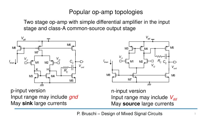
Popular op-amp topologies Two stage op-amp with simple differential amplifier in the input stage and class-A common-source output stage p-input version Input range may include gnd May sink large currents n-input version Input range may include Vdd May source large currents P. Bruschi Design of Mixed Signal Circuits 1
Improved topologies (better performances, but greater complexity) Class AB stages Cascode stages Large output current with small quiescent power consumption Larger gain, simpler Rail- to-Rail input stages P. Bruschi Design of Mixed Signal Circuits 2
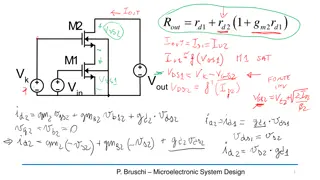
Class-AB output stages ????? Quiescent currents: ( V 1 2 = 5 7 I I ID5does not depend on Vdd, while ID6does. The output short circuit current depends on Vdd 5 D bias 3 8 ) 2 = = V V V V 6 I V Poor PSRR 6 5 GS DD batt GS 6 6 D GS tp 2 P. Bruschi Design of Mixed Signal Circuits 3
Op-amps with class- AB output stages If we want to save this solution, we need to adapt both VGS5and VGS6when Vddchanges, and guarantee that: I I = 5 6 D D is always valid P. Bruschi Design of Mixed Signal Circuits 4
Op-amps with class- AB output stages Bias chain Voltage shifter ( ) 2 = 6 I V V 6 6 D GS tp 2 IB = V V V V 6 10 3 GS DD GS GS = V V V V 22 21 20 GS DD GS GS I I = 20 B = 21 B I I = V V 3 3 D Good PSRR 10 10 D 6 22 GS GS P. Bruschi Design of Mixed Signal Circuits 5
Op-amps with class- AB output stages Second stage Second stage Voltage shifter: additional singularities Ym2(s) Gm2(s) Gm2=gm5+gm6 P. Bruschi Design of Mixed Signal Circuits 6
Limitations: minimum Vdd For the class-A amplifier, the minimum Vdd was only VGS+2VDSAT 0.9 V Minimum Vdd: 3VGS 2.1 V P. Bruschi Design of Mixed Signal Circuits 7
Reduced VGSexcursion for the output devices ( ) 2 = 6 I V V OP MAX 6 GS MAX tp 2 ( ) 2 = 5 I V V ON MAX 5 GS MAX tn 2 Both VGS5and VGS6cannot reach Vdd. If large output currents are required, this means that M5 and M6 should be designed with very large W ION-MAXstrongly depends on the input common mode voltage = + V V V DSAT V 5 GS MAX iC GS = V V V 6 10 GS MAX dd GS P. Bruschi Design of Mixed Signal Circuits 8
The Monticelli's class-AB stage Ihand Ikincludes also the variations due to the input signal and have a high output differential resistance (not shown for simplicity) p n InIp = I I const h k + + 0 i i I I const n p p n Floating battery = = i g v i g v n mMN = gn p mMP gp g v g v mMN gn mMP gp v v g g gn = mMP D. M. Monticelli, A qu d C OS in l -supply op amp with rail-to-rail ou pu win , IEEE J. Solid-State Circuits, vol. SC-21, pp. 1026-1034, Dec. 1986. gp mMN P. Bruschi Design of Mixed Signal Circuits 9
The Monticelli's class-AB stage p n Here, Ip>>In, then vgn>>vgp and VBreduces VB VBN output devices MNMand MMP, are designed to have same gmin the operating point: vgn=vgp (variations) v v g g gn = mMP = I 2 g m D gp mMN P. Bruschi Design of Mixed Signal Circuits 10
First stage: folded cascode for improved gain and larger swing n-input folded cascode Folded cascode with rail-to-rail input range P. Bruschi Design of Mixed Signal Circuits 11
High performance - two-stage CMOS op-amp 3 High gain: ???? Class-AB output stage Rail-to-Rail input range M24 and M35 form the Monticelli's cell M22-M23 and M33-M34 produce the gate bias for M24 and M35, respectively In quiescent conditions, we design Ibias, M23 and M34 to make: VGS24=VGS23and VGS35=VGS34 Minimum Vdd: 2VGS+VDSAT 1.5 V This simplify setting of M1,M2 quiescent current = = V V V V 1 22 GS GS R. Hogervorst l., A Compact Power-Efficient 3 V CMOS Rail-to-Rail Inpu /Ou pu Op r ion l Amplifi r for VLSI C ll Libr ri , IEEE JSSC, 99 2 33 GS GS P. Bruschi Design of Mixed Signal Circuits 12
Commercial products P. Bruschi Design of Mixed Signal Circuits 13