Nanoscience and Nanotechnology with Dr. Abeer Alshammari
DR.ABEER ALSHAMMARI 2021
1
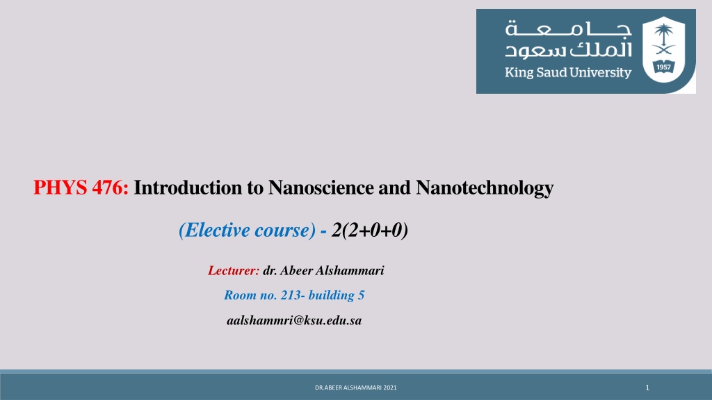
PHYS 476:
Introduction to Nanoscience and Nanotechnology
(Elective course) -
2(2+0+0)
Lecturer:
dr. Abeer Alshammari
Room no. 213- building 5
a
alshammri@ksu.edu.sa
Unique Properties of Nanomaterials
2.1 Microstructure and defects in nanocrystalline materials
2.2 Effect of nano-dimensions on materials behaviour
2.1.1 Dislocations
2.1.2 Twins, stacking faults and voids
2.1.3 Grain boundaries, triple junctions and disclinations
2.2.1 Elastic properties
2.2.2 Melting point
2.2.3 Diffusivity
2.2.4 Grain growth characteristics
2.2.5 Enhanced solid solubility
2.2.6 Magnetic properties
2.2.7 Electrical properties
2.2.8 Optical properties
2.2.9 Thermal properties
2.2.10 Mechanical properties
DR.ABEER ALSHAMMARI 2021
2
2.1 MICROSTRUCTURE AND DEFECTS IN NANOCRYSTALLINE MATERIALS
The microstructural features of importance in nanomaterials include:
• Grain size, distribution and morphology
• The nature of grain boundaries and interphase interfaces
• Nature of intragrain defects
• Composition profiles across grains and interfaces
• Residual impurities from processing
Crystal lattice imperfections, such as point, linear, planar and volume defects, lead to the structure-sensitive properties of
materials.
In order to understand the novel properties of nanostructured
materials, we need to understand the structure and its inter -
relationship with properties.
Crystals are three-dimensional, periodic arrangements of
atoms/molecules in space.
Any imperfection leading to disruption of periodicity is referred to as
a ‘crystalline defect’. These defects are usually classified based on
their dimensionality, namely, point defects (0D), line defects (1D),
surface defects (2D) and volume defects (3D).
DR.ABEER ALSHAMMARI 2021
3
2.1.1 Dislocations
•
Missing rows of atoms in a crystal are regions of high energy and stress due to disruption of the atomic bonds in the plane.
This provides a driving force for dislocations to be annihilated at surfaces or grain boundaries to minimize the strain energy
of the crystal.
•
Line defects (one dimensional defects), or dislocations, are
lines along which whole rows of atoms in a solid are arranged
anomalously. The resulting irregularity in spacing is most
severe along a line called the line of dislocation. Dislocation is
perhaps the most important crystalline defect , they can
weaken or strengthen solids.
W
ith decreasing grain size of nanograined materials, dislocation stability is reduced, due to the large grain boundary area.
•
The typical dislocation density in annealed crystalline materials is about 10
10
/cm. As the grain size is reduced to about 10
nm, the dislocation density can reduce by 2–3 orders or more and finally, below a critical grain size, dislocations are no
longer stable, i.e., there will be no dislocations in the nanocrystalline materials below the critical grain size.
The behaviour of nanocrystalline materials is decided to a large extent by these defects, and as such, nanomaterials exhibit
vastly different properties compared to bulk materials.
DR.ABEER ALSHAMMARI 2021
4
2.1.2 Twins, stacking faults and voids
•
planar defects are often observed, even after annealing, in many faceted nanomaterials, including nano rods and
nanowires. These planar defects include twins and stacking faults (intrinsic or extrinsic), and are usually neglected by most
analytical models.
For example, many bulk metals have the face-centred cubic structure, but nanocrystals
and nanorods of the same material often exhibit various structural modifications such
as single or multiple symmetric twinning, as well as five-fold cyclic twinning, resulting
in decahedral and truncated decahedral nanostructures below critical sides.
•
Twins are generally observed in crystals subjected to deformation under high strain
rate or at low temperatures. During crystallization of liquid metal, it is expected that
volume misfit strains can be easily accommodated in the liquid phase, and hence one
does not expect the formation of twins in the nucleating crystals.
DR.ABEER ALSHAMMARI 2021
5
Voids in nanocrystallites may be located at either
Triple junctions
Large porosities
Due to insufficient compaction and sintering of nanocrystallites
synthesized from the powder method. Although both types of voids
influence the behaviour of the nanocrystallites, the first is structurally
more important. It is suggested that triple junction voids arise as a result of
relaxation of nanocrystalline grain boundaries.
2.1.3 Grain boundaries, triple junctions and disclinations
A schematic representation of a hard-sphere model of an equiaxed nanocrystalline
metal as shown in Figure.
Two types of atoms can be distinguished:
Crystal atoms with nearest-neighbour configurations corresponding to the lattice
(black circles) .
Boundary atoms with a variety of interatomic spacings (white circles).
Nanocrystalline materials typically contain a high number of interfaces with
random orientation relationships, so, a substantial fraction of atoms lies in the
interfaces.
DR.ABEER ALSHAMMARI 2021
6
DR.ABEER ALSHAMMARI 2021
7
Assuming that the grains have the shape of spheres or cubes, the volume fraction of nanocrystalline materials
associated with the boundaries (Vi) is estimated to be:
where δ is the average interface thickness and d is the average grain diameter. Thus, the volume fraction of
interfaces can be as much as 60% for 5 nm grains, 30% for 10 nm grains, and about 3% for 100 nm grains, for a
grain boundary thickness of 1 nm.
When the grain size is smaller than about 20 nm, the total volume of the intercrystalline region
(grain boundary and triple junctions) becomes significant. The density of grain boundaries in
nanocrystals is very large (~ 1019 cm–3) and there is wide distribution of interatomic spacing at
these grain boundaries.
It has been suggested that the triple junctions can be described based on the disclination defect
model. Disclinations (as Figure) are line defects characterised by a rotation vector ω in contrast to
the translational vector b for dislocations.
The triple junctions may be considered to form a network of disclinations. Theoretical calculations
have shown that triple junction energies are comparable to dislocation energies, and that
compensating disclinations play a significant role in the properties of nanocrystalline metals with
grain size less than about 10 nm. These triple junctions are linear defects that play a significant role
in the mechanical, thermodynamic and kinetic properties of polycrystals.
DR.ABEER ALSHAMMARI 2021
8
2.2 EFFECT OF NANO-DIMENSIONS ON MATERIALS BEHAVIOUR
2.2.1 Elastic properties
•
The elastic modulus of a material is proportional to the bond strength between atoms or
molecules. The higher the bond strength, the higher will be the melting point and elastic
modulus
•
The elastic properties of crystalline materials are usually considered to be structure
(microstructure) independent.
•
If the temperature is increased, the mean separation between atoms increases and
the elastic modulus decreases. A large increase in vacancy and other defect concentrations can
be treated as equivalent to higher apparent temperature. Increasing the defect concentration is
thus expected to decrease the elastic modulus
•
Nanomaterials, by virtue of their very high defect concentration, may have considerably lower
elastic properties in comparison to bulk materials. The elastic modulus of nanocrystalline
compacts was found to be 30%–50% lower than bulk values.
•
T
he porosities in the compact due to inadequate sintering can also influence the measured elastic properties. In contrast to
nanograined materials, it has been suggested that the elastic modulus of carbon nanotubes increases with decrease in tube
diameter. The increase of apparent elastic modulus for smaller diameters is attributed to the surface tension effects.
•
The effect of porosities on the elastic modulus is particularly predominant in materials
with grain size below ~ 20 nm. The presence of porosities can result in a decrease in
modulus of up to 20%–25%
DR.ABEER ALSHAMMARI 2021
9
2.2.2 Melting point
T
he decrease in bonding energy due to enhanced surface and grain boundary area in nanocrystalline materials can
reduce the enthalpy of fusion and the melting temperature. At the melting point of a material, the solid and liquid
phases are in equilibrium.
T
he change in melting temperature is inversely proportional to the radius of the sphere. In other words, as the grain
size is reduced, the melting point is lowered.
It has been observed that nano-CdS of diameter ~ 2.5 nm melts at 600 K, much lower than the bulk melting point
(1675 K). The single-walled carbon nanotube melts at ~ 1600 K, 0.42 times its bulk melting point (3800 K).
It is known that atoms in a solid vibrate about their mean position. The amplitude of the vibrations increases with
increasing temperature. When the vibration amplitude exceeds a certain percentage of the bond length, melting
begins at the surface and propagates through the solid. Atoms at the surface and grain boundary are less constrained
to vibrate compared to atoms inside the crystal lattice. As the grain size decreases, the percentage of atoms residing
at surfaces and grain boundaries increases significantly. Hence, freestanding nanoparticles may show a lower melting
point compared to bulk.
A similar effect has been reported on zinc nanowires embedded in holes in an anodic alumina membrane.
The melting point of zinc nanowires was found to decrease with decreasing diameter of the nanowire.
DR.ABEER ALSHAMMARI 2021
10
It is fascinating to observe that the melting temperature does not continuously decrease with decreasing grain size in nano-
dimensions. In fact, as the cluster size is reduced below a critical limit, the melting point of clusters is seen to increase above
the bulk melting temperature of the material, at least in some cases.
It has been found that a solid containing about 10 atoms of Ga or IV A elements (C, Si, Ge, Sn and Pb) melts at temperatures
that are higher than the melting point of the corresponding bulk solid.
In contrast to nanoclusters and nano-agglomerates,
nanoparticles within a matrix may, in fact, experience an
enhancement in the melting temperature.
T
he melting point of nanoparticles embedded in a bulk matrix
increases with decreasing size of particulate as the pressure increases
with decrease in particle size. It was found that Ge nanocrystals
embedded in silica glass do not melt until temperatures are almost
200°C above the melting point of bulk Ge, and resolidify only when
the temperature is more than 200°C below its bulk melting point.
Delve into the fascinating world of nanoscience and nanotechnology through the elective course PHYS 476 with Dr. Abeer Alshammari. Learn about the unique properties of nanomaterials, including microstructure, defects, dislocations, twins, stacking faults, and more. Discover how nano-dimensions impact material behavior, such as elastic properties and melting points, and explore the exciting realm of magnetic, electrical, optical, thermal, and mechanical properties at the nanoscale.

Download Presentation

Please find below an Image/Link to download the presentation.
The content on the website is provided AS IS for your information and personal use only. It may not be sold, licensed, or shared on other websites without obtaining consent from the author.If you encounter any issues during the download, it is possible that the publisher has removed the file from their server.
You are allowed to download the files provided on this website for personal or commercial use, subject to the condition that they are used lawfully. All files are the property of their respective owners.
The content on the website is provided AS IS for your information and personal use only. It may not be sold, licensed, or shared on other websites without obtaining consent from the author.
E N D
Presentation Transcript
PHYS 476: Introduction to Nanoscience and Nanotechnology (Elective course) - 2(2+0+0) Lecturer: dr. Abeer Alshammari Room no. 213- building 5 aalshammri@ksu.edu.sa 1 DR.ABEER ALSHAMMARI 2021
Unique Properties of Nanomaterials 2.1 Microstructure and defects in nanocrystalline materials 2.1.3 Grain boundaries, triple junctions and disclinations 2.1.1 Dislocations 2.1.2 Twins, stacking faults and voids 2.2 Effect of nano-dimensions on materials behaviour 2.2.6 Magnetic properties 2.2.1 Elastic properties 2.2.2 Melting point 2.2.7 Electrical properties 2.2.3 Diffusivity 2.2.8 Optical properties 2.2.4 Grain growth characteristics 2.2.9 Thermal properties 2.2.10 Mechanical properties 2.2.5 Enhanced solid solubility 2 DR.ABEER ALSHAMMARI 2021
2.1 MICROSTRUCTURE AND DEFECTS IN NANOCRYSTALLINE MATERIALS 3 DR.ABEER ALSHAMMARI 2021
2.1.1 Dislocations Line defects (one dimensional defects), or dislocations, are lines along which whole rows of atoms in a solid are arranged anomalously. The resulting irregularity in spacing is most severe along a line called the line of dislocation. Dislocation is perhaps the most important crystalline defect , they can weaken or strengthen solids. 4 DR.ABEER ALSHAMMARI 2021
2.1.2 Twins, stacking faults and voids 5 DR.ABEER ALSHAMMARI 2021
2.1.3 Grain boundaries, triple junctions and disclinations 6 DR.ABEER ALSHAMMARI 2021
7 DR.ABEER ALSHAMMARI 2021
2.2 EFFECT OF NANO-DIMENSIONS ON MATERIALS BEHAVIOUR 2.2.1 Elastic properties 8 DR.ABEER ALSHAMMARI 2021
2.2.2 Melting point 9 DR.ABEER ALSHAMMARI 2021